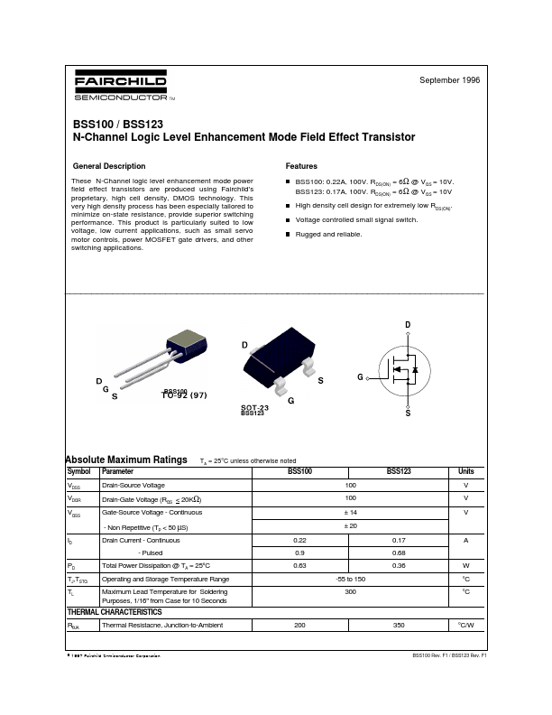
Datasheet4U Logo Datasheet4U.com

BSS100 - N-Channel Logic Level Enhancement Mode Field Effect Transistor

General Description

These N-Channel logic level enhancement mode power field effect transistors are produced using Fairchild's proprietary, high cell density, DMOS technology.

This very high density process has been especially tailored to minimize on-state resistance, provide superior switching performance.

Key Features

  • BSS100: 0.22A, 100V. RDS(ON) = 6Ω @ VGS = 10V. BSS123: 0.17A, 100V. RDS(ON) = 6Ω @ VGS = 10V High density cell design for extremely low RDS(ON). Voltage controlled small signal switch. Rugged and reliable. _______________________________________________________________________________ D G BSS100 BSS123 S Absolute Maximum Ratings Symbol Parameter TA = 25°C unless otherwise noted BSS100 BSS123 Units VDSS VDGR VGSS Drain-Source Voltage Drain-Gate Voltage (RGS < 20KΩ) Gate-Source Voltage.

📥 Download Datasheet

Full PDF Text Transcription (Reference)

The following content is an automatically extracted verbatim text from the original manufacturer datasheet and is provided for reference purposes only.

View original datasheet text
September 1996 BSS100 / BSS123 N-Channel Logic Level Enhancement Mode Field Effect Transistor General Description These N-Channel logic level enhancement mode power field effect transistors are produced using Fairchild's proprietary, high cell density, DMOS technology. This very high density process has been especially tailored to minimize on-state resistance, provide superior switching performance. This product is particularly suited to low voltage, low current applications, such as small servo motor controls, power MOSFET gate drivers, and other switching applications. Features BSS100: 0.22A, 100V. RDS(ON) = 6Ω @ VGS = 10V. BSS123: 0.17A, 100V. RDS(ON) = 6Ω @ VGS = 10V High density cell design for extremely low RDS(ON). Voltage controlled small signal switch. Rugged and reliable.