CD4049UBC
Description
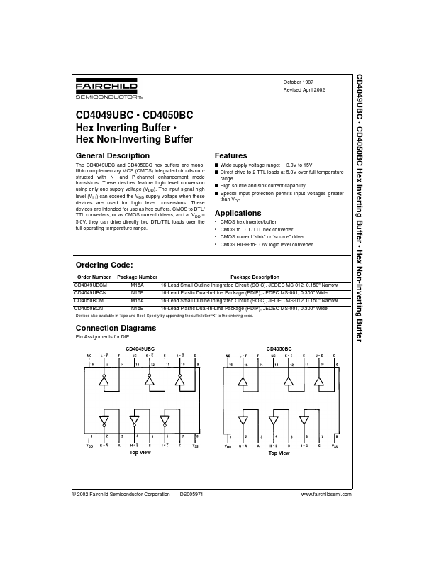
The CD4049UBC and CD4050BC hex buffers are monolithic plementary MOS (CMOS) integrated circuits constructed with N- and P-channel enhancement mode transistors.
Applications
- CMOS to DTL/TTL hex converter
The CD4049UBC and CD4050BC hex buffers are monolithic plementary MOS (CMOS) integrated circuits constructed with N- and P-channel enhancement mode transistors.
| Part Number | Manufacturer | Description |
|---|---|---|
| CD4049UBC | National Semiconductor | Hex Inverting/Non-Inverting Buffer |
| CD4049UBM | National Semiconductor | Hex Inverting/Non-Inverting Buffer |
| CD4049UBM | Texas Instruments | CMOS Hex Inverting Buffer/Converter |
| CD4049UBE | Texas Instruments | CMOS Hex Inverting Buffer/Converter |
| CD4049UB | Texas Instruments | CMOS Hex Inverting Buffer/Converter |
| CD4049UB | Harris Corporation | CMOS Hex Buffer/Converters |
| CD4049UBF | Texas Instruments | CMOS Hex Inverting Buffer/Converter |
| CD4049UBF3A | Texas Instruments | CMOS Hex Inverting Buffer/Converter |
| CD4049UBMS | Intersil | CMOS Hex Buffer/Converter |
| CD4049UB | RCA | CMOS HEX BUFFERS/CONVERTERS |