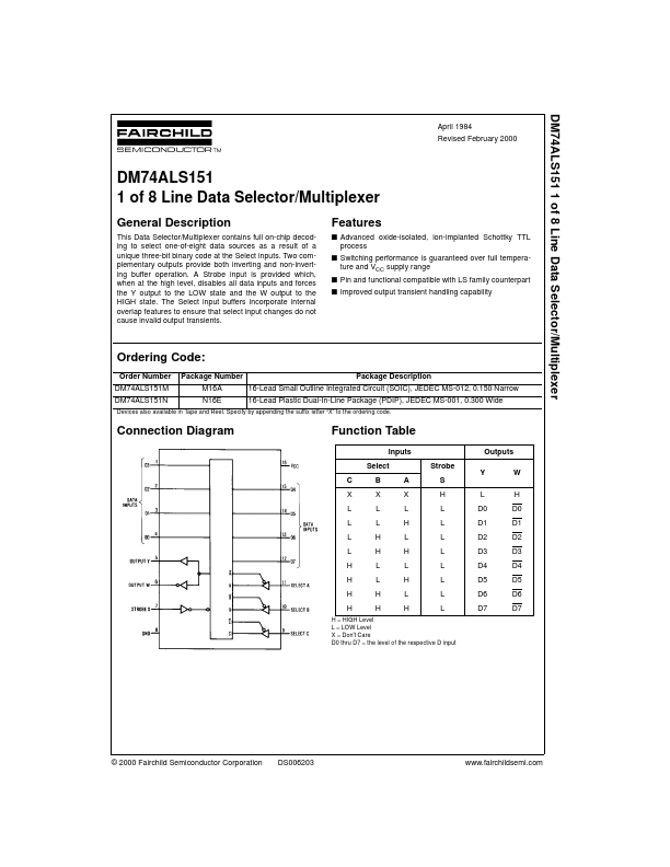
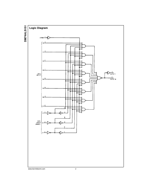
GENERAL DESCRIPTION
Two complementary outputs provide both inverting and non-inverting buffer operation. A Strobe input is provided which, when at the high level, disables all data inputs and forces the Y output to the LOW state and the W output to the HIGH state. FEATURES
s Advanced oxide-isolated, ion-implanted Schottky TTL process s Switching performance is guaranteed over full temperature and VCC supply range s Pin and functional compatible with LS family counterpart s Improved output transient handling capability Ordering Code: Order Number DM74ALS151M DM74ALS151N Package Number M16A N16E Package DESCRIPTION
16-Lead Small Outline Integrated Circuit (SOIC), JEDEC MS-012, 0.150 Narrow 16-Lead Plastic Dual-In-Line Package (PDIP), JEDEC MS-001, 0.300 Wide Devices also available in Tape and Reel. Specify by appending the suffix letter “X” to the ordering code. Connection Diagram Function Table Inputs Select C X L L L L H H H H B X L L H H L L H H A X L H L H L H L H Strobe Y S H L L L... Fairchild Semiconductor