DM74LS112A
DM74LS112A is Dual Negative-Edge-Triggered Master-Slave J-K Flip-Flop manufactured by Fairchild Semiconductor.
Description
This device contains two independent negative-edge-triggered J-K flip-flops with plementary outputs. The J and K data is processed by the flip-flop on the falling edge of the clock pulse. The clock triggering occurs at a voltage level and is not directly related to the transition time of the falling edge of the clock pulse. Data on the J and K inputs may be changed while the clock is HIGH or LOW without affecting the outputs as long as the setup and hold times are not violated. A low logic level on the preset or clear inputs will set or reset the outputs regardless of the logic levels of the other inputs.
Ordering Code:
Order Number DM74KS112AM DM74LS112AN Package Number M16A N16E Package Description 16-Lead Small Outline Integrated Circuit (SOIC), JEDEC MS-012, 0.150 Narrow 16-Lead Plastic Dual-In-Line Package (PDIP), JEDEC MS-001, 0.300 Wide
Devices also available in Tape and Reel. Specify by appending the suffix letter “X” to the ordering code.
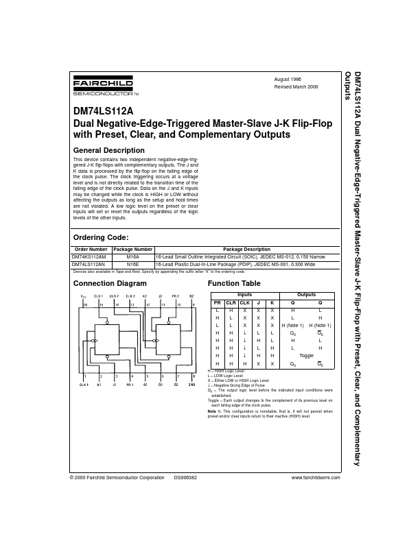
Connection Diagram
Function Table
Inputs PR L H L H H H H H CLR CLK H L L H H H H H X X X ↓ ↓ ↓ ↓ H J X X X L H L H X K X X X L L H H X Q0 Q H L H (Note 1) Q0 H L Toggle Q0 Outputs Q L H H (Note 1) Q0 L H
H = HIGH Logic Level L = LOW Logic Level X = Either LOW or HIGH Logic Level ↓ = Negative Going Edge of Pulse Q0 = The output logic level before the indicated input conditions were established. Toggle = Each output changes to the plement of its previous level on each falling edge of the clock pulse. Note 1: This configuration is nonstable; that is, it will not persist when preset and/or clear inputs return to their inactive (HIGH) level.
© 2000 Fairchild Semiconductor Corporation
DS006382
.fairchildsemi.
Absolute Maximum Ratings(Note 2)
Supply Voltage Input Voltage Operating Free Air Temperature Range Storage Temperature Range 7V 7V 0°C to +70°C
- 65°C to +150°C
Note 2: The “Absolute Maximum Ratings” are those values beyond which the safety of the device cannot be guaranteed. The device...