DM74LS273
DM74LS273 is 8-Bit Register manufactured by Fairchild Semiconductor.
Description
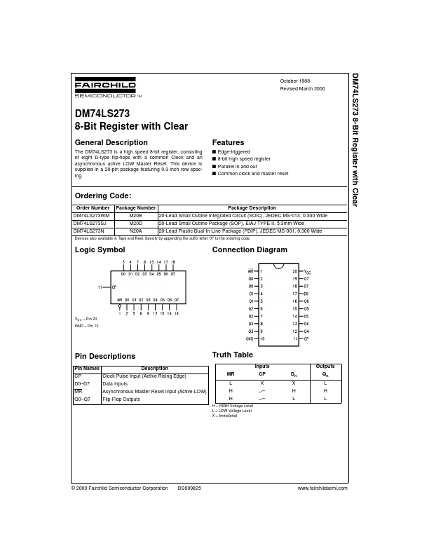
The DM74LS273 is a high speed 8-bit register, consisting of eight D-type flip-flops with a mon Clock and an asynchronous active LOW Master Reset. This device is supplied in a 20-pin package featuring 0.3 inch row spacing.
Features s Edge-triggered s 8-bit high speed register s Parallel in and out s mon clock and master reset
Ordering Code:
Order Number DM74LS273WM DM74LS273SJ DM74LS273N Package Number M20B M20D N20A Package Description
20-Lead Small Outline Integrated Circuit (SOIC), JEDEC MS-013, 0.300 Wide 20-Lead Small Outline Package (SOP), EIAJ TYPE II, 5.3mm Wide 20-Lead Plastic Dual-In-Line Package (PDIP), JEDEC MS-001, 0.300 Wide
Devices also available in Tape and Reel. Specify by appending the suffix letter “X” to the ordering code.
Logic Symbol
Connection Diagram
VCC = Pin 20 GND = Pin 10
Pin Descriptions
Pin Names CP D0- D7 MR Q0- Q7 Data Inputs Asynchronous Master Reset Input (Active LOW) Flip-Flop Outputs Description
Clock Pulse Input (Active Rising Edge)
Truth Table
Inputs MR L H H
H = HIGH Voltage Level L = LOW Voltage Level X = Immaterial
Outputs Dn X H L Qn L H L
© 2000 Fairchild Semiconductor Corporation
DS009825
.fairchildsemi.
Functional Description
The DM74LS273 is an 8-bit parallel register with a mon Clock and mon Master Reset. When the MR input is LOW, the Q outputs are LOW, independent of the other inputs. Information meeting the setup and hold time requirements of the D inputs is transferred to the Q outputs on the LOW-to-HIGH transition of the clock input.
Logic Diagram
.fairchildsemi.
Absolute Maximum Ratings(Note 1)
Supply Voltage Input Voltage Operating Free Air Temperature Range Storage Temperature Range 7V 7V 0°C to +70°C
- 65°C to +150°C
Note 1: The “Absolute Maximum Ratings” are those values beyond which the safety of the device cannot be guaranteed. The device should not be operated at these limits. The parametric values defined in the Electrical Characteristics tables...