DM81LS97A
Description
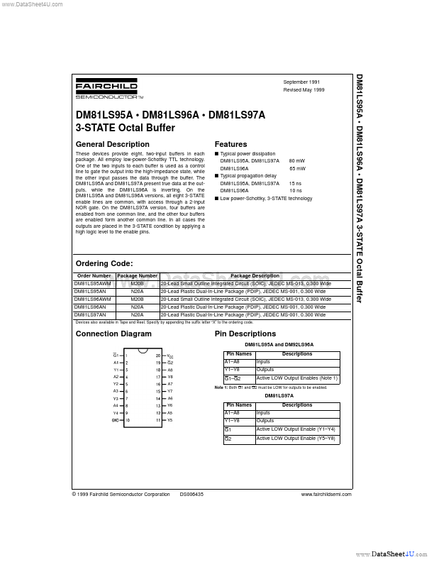
These devices provide eight, two-input buffers in each package. All employ low-power-Schottky TTL technology. One of the two inputs to each buffer is used as a control line to gate the output into the high-impedance state, while the other input passes the data through the buffer. The DM81LS95A and DM81LS97A present true data at the outputs, while the DM81LS96A is inverting. On the DM81LS95A and DM81LS96A versions, all eight 3-STATE enable lines are mon, with access through a 2-input NOR gate. On the DM81LS97A version, four buffers are enabled from one mon line, and the other four buffers are enabled form another mon line. In all cases the outputs are placed in the 3-STATE condition by applying a high logic level to the enable pins.
Features s Typical power dissipation DM81LS95A, DM81LS97A DM81LS96A s Typical propagation delay DM81LS95A, DM81LS97A DM81LS96A 15 ns 10 ns 80 m W 65 m W s Low power-Schottky, 3-STATE technology
Ordering Code:
Order Number DM81LS95AN DM81LS96AN...