FAN48632
Overview
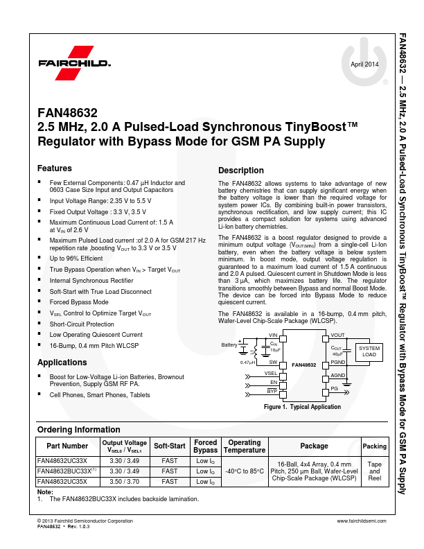
The FAN48632 allows systems to take advantage of new battery chemistries that can supply significant energy when the battery voltage is lower than the required voltage for system power ICs. By combining built-in power transistors, synchronous rectification, and low supply current; this IC provides a compact solution for systems using advanced Li-Ion battery chemistries.
- Few External Components: 0.47 µH Inductor and 0603 Case Size Input and Output Capacitors
- Input Voltage Range: 2.35 V to 5.5 V
- Fixed Output Voltage : 3.3 V, 3.5 V
- Maximum Continuous Load Current of: 1.5 A at VIN of 2.6 V
- Maximum Pulsed Load current :of 2.0 A for GSM 217 Hz repetition rate ,boosting VOUT to 3.3 V or 3.5 V
- Up to 96% Efficient
- True Bypass Operation when VIN > Target VOUT
- Internal Synchronous Rectifier
- Soft-Start with True Load Disconnect
- Forced Bypass Mode