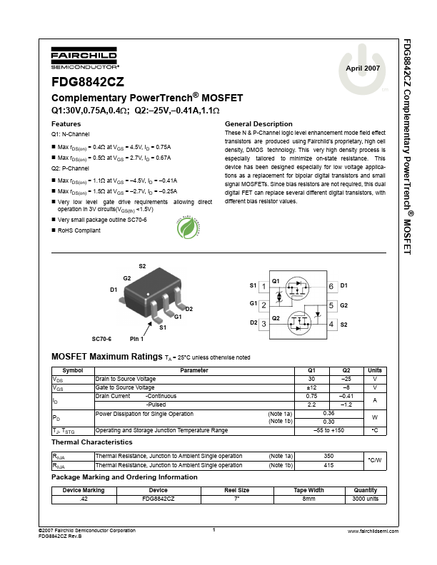
FDG8842CZ
Features
Q1: N-Channel
- Max r DS(on) = 0.4Ω at VGS = 4.5V, ID = 0.75A
- Max r DS(on) = 0.5Ω at VGS = 2.7V, ID = 0.67A Q2: P-Channel
- Max r DS(on) = 1.1Ω at VGS =
- 4.5V, ID =
- 0.41A
- Max r DS(on) = 1.5Ω at VGS =
- 2.7V, ID =
- 0.25A
- Very low level gate drive requirements allowing direct operation in 3V circuits(VGS(th) <1.5V)
- Very small package outline SC70-6
General Description
These N & P-Channel logic level enhancement mode field effect transistors are produced using Fairchild’s proprietary, high cell density, DMOS technology. This very high density process is especially tailored to minimize on-state resistance. This device has been designed especially for low voltage applications as a replacement for bipolar digital transistors and small signal MOSFETs. Since bias resistors are not required, this dual digital...