FDMA1430JP
Features
- Max r DS(on) = 90 mΩ at VGS = -4.5 V, ID = -2.9 A
- Max r DS(on) = 130 mΩ at VGS = -2.5 V, ID = -2.6 A
- Max r DS(on) = 170 mΩ at VGS = -1.8 V, ID = -1.7 A
- Max r DS(on) = 240 mΩ at VGS = -1.5 V, ID = -1 A
- Low profile
- 0.8 mm maximum
- in the new package
Micro FET 2x2
- HBM ESD protection level > 2 k V typical (Note 3)
- Ro HS pliant
General Description
This device is designed specifically as a single package solution for loadswitching in cellular handset and other ultra-portable applications. It features a 50 V NPN BJT and a 30 V P-ch Trench MOSFET in the space saving Micro FET 2x2 package that offers exceptional thermal performance for it's physical size and is well suited to linear mode applications.
Application
- Loadswitching
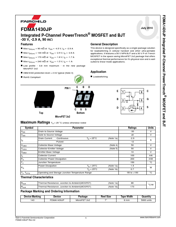
PIN 1
E BD
C GS
Top
Bottom
Micro FET 2x2
Maximum Ratings TA = 25 °C unless otherwise noted
Symbol VDS VGS
VCBO VCEO VEBO IC PC TJ
TJ, TSTG
Parameter
Drain to Source Voltage
Gate to Source Voltage
Drain Current...