Datasheet4U Logo Datasheet4U.com

FDMA86265P Datasheet P-channel MOSFET

Manufacturer: Fairchild (now onsemi)

Overview: FDMA86265P P-Channel PowerTrench® MOSFET August 2018 FDMA86265P P-Channel PowerTrench® MOSFET -150 V, -1 A, 1.

General Description

This P-Channel MOSFET is produced using Fairchild Semiconductor‘s advanced PowerTrench® process that has been optimized for the on-state resistance and yet maintain superior switching performance.

Applications „ Active Clamp Switch „ Load Switch Pin 1 Drain DD G Source BBootttotomm DDraraininCCoonnta- ct DD DD DD S MicroFET 2X2 (Bottom View) G S MOSFET Maximum Ratings TA = 25 °C unless otherwise noted Symbol VDS VGS ID EAS PD TJ, TSTG Parameter Drain to Source Voltage Gate to Source Voltage Drain Current -Continuous -Pulsed TA = 25 °C Single Pulse Avalanche Energy Power Dissipation TA = 25 °C Power Dissipation TA = 25 °C Operating and Storage Junction Temperature Range Thermal Characteristics (Note 1a) (Note 3) (Note 1a) (Note 1b) Ratings -150 ±25 -1 -2 6 2.4 0.9 -55 to + 150 Units V V A mJ W °C RθJA RθJA Thermal Resistance, Junction to Ambient Thermal Resistance, Junction to Ambient Package Marking and Ordering Information (Note 1a) (Note 1b) 52 145 °C/W Device Marking 265 Device FDMA86265P Package MicroFET 2X2 Reel Size 7 ’’ Tape Width 12 mm Quantity 3000 units ©2014 Semiconductor ponents Industries, LLC FDMA86265P Rev.2 1 .onsemi.

FDMA86265P P-Channel PowerTrench® MOSFET Electrical Characteristics TJ = 25 °C unless otherwise noted Symbol Parameter Test Conditions Min Typ Max Units Off Characteristics BVDSS ΔBVDSS ΔTJ IDSS IGSS Drain to Source Breakdown Voltage Breakdown Voltage Temperature Coeffic

Key Features

  • Max rDS(on) = 1.2 Ω at VGS = -10 V, ID = -1 A.
  • Max rDS(on) = 1.4 Ω at VGS = -6 V, ID = -0.9 A.
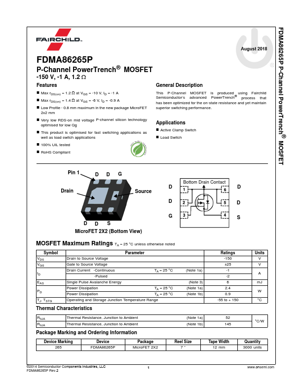
  • Low Profile - 0.8 mm maximum in the new package MicroFET 2x2 mm.
  • Very low RDS-on mid voltage P-channel silicon technology optimised for low Qg.
  • This product is optimised for fast switching.

FDMA86265P Distributor