FDMS6673BZ
Features
General Description
- Max r DS(on) = 6.8 m: at VGS = -10 V, ID = -15.2 A
- Max r DS(on) = 12.5 m: at VGS = -4.5 V, ID = -11.2 A
- Advanced Package and Silicon bination for Low r DS(on)
- HBM ESD Protection Level of 8 k V Typical(Note 3)
- MSL1 Robust Package Design
- Ro HS pliant
The FDMS6673BZ has been designed to minimize losses in load switch applications. Advancements in both silicon and package technologies have been bined to offer the lowest r DS(on) and ESD protection.
Applications
- Load Switch in Notebook and Server
- Notebook Battery Pack Power Management
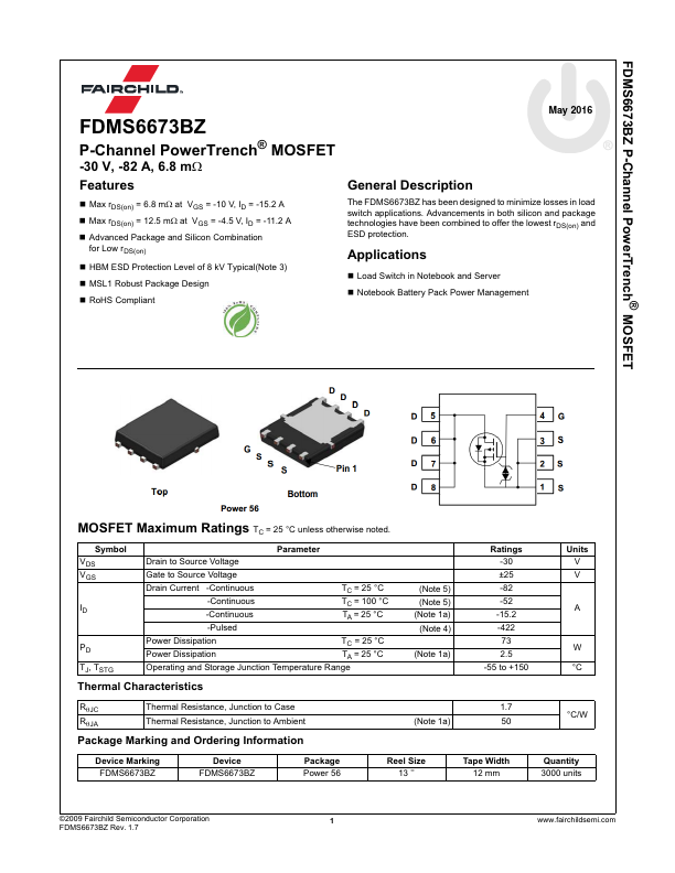
D 55
D 66
Pin 1
D7 D 88
Top
Bottom
Power 56
44 G 33 S 22 S 11 S
MOSFET Maximum Ratings TC = 25 °C unless otherwise noted.
Symbol VDS VGS
PD TJ, TSTG
Parameter
Drain to Source Voltage
Gate to Source Voltage
Drain Current -Continuous -Continuous -Continuous -Pulsed
TC = 25 °C TC = 100 °C TA = 25 °C
Power Dissipation
TC = 25 °C
Power Dissipation
TA = 25 °C
Operating and Storage...