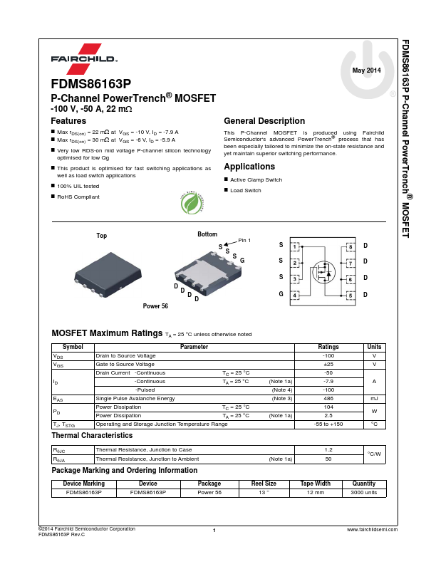
Datasheet4U Logo Datasheet4U.com

FDMS86163P Datasheet P-Channel PowerTrench MOSFET

Manufacturer: Fairchild (now onsemi)

General Description

This P-Channel MOSFET is produced using Fairchild Semiconductor‘s advanced PowerTrench® process that has been especially tailored to minimize the on-state resistance and yet maintain superior switching performance.

Applications „ Active Clamp Switch „ Load Switch Top Bottom Pin 1 SS S S GS Power 56 D D D D S G D D D D MOSFET Maximum Ratings TA = 25 °C unless otherwise noted Symbol VDS VGS ID EAS PD TJ, TSTG Parameter Drain to Source Voltage Gate to Source Voltage Drain Current -Continuous -Continuous -Pulsed TC = 25 °C TA = 25 °C Single Pulse Avalanche Energy Power Dissipation TC = 25 °C Power Dissipation TA = 25 °C Operating and Storage Junction Temperature Range Thermal Characteristics (Note 1a) (Note 4) (Note 3) (Note 1a) Ratings -100 ±25 -50 -7.9 -100 486 104 2.5 -55 to +150 Units V V A mJ W °C RθJC RθJA Thermal Resistance, Junction to Case Thermal Resistance, Junction to Ambient Package Marking and Ordering Information (Note 1a) 1.2 50 °C/W Device Marking FDMS86163P Device FDMS86163P Package Power 56 Reel Size 13 ’’ Tape Width 12 mm Quantity 3000 units ©2014 Fairchild Semiconductor Corporation FDMS86163P Rev.C 1 www.fairchildsemi.com FDMS86163P P-Channel PowerTrench® MOSFET Electrical Characteristics TJ = 25 °C unless otherwise noted Symbol Parameter Test Conditions Min Typ Max Units Off Characteristics BVDSS ΔBVDSS ΔTJ IDSS IGSS Drain to Source Breakdown Voltage Breakdown Voltage Temperature Coefficient Zero Gate Voltage Drain Current Gate to Source Leakage Current ID =

Overview

FDMS86163P P-Channel PowerTrench® MOSFET FDMS86163P P-Channel PowerTrench® MOSFET -100 V, -50 A, 22.

Key Features

  • Max rDS(on) = 22 mΩ at VGS = -10 V, ID = -7.9 A.
  • Max rDS(on) = 30 mΩ at VGS = -6 V, ID = -5.9 A.
  • Very low RDS-on mid voltage P-channel silicon technology optimised for low Qg.
  • This product is optimised for fast switching.