Datasheet Summary
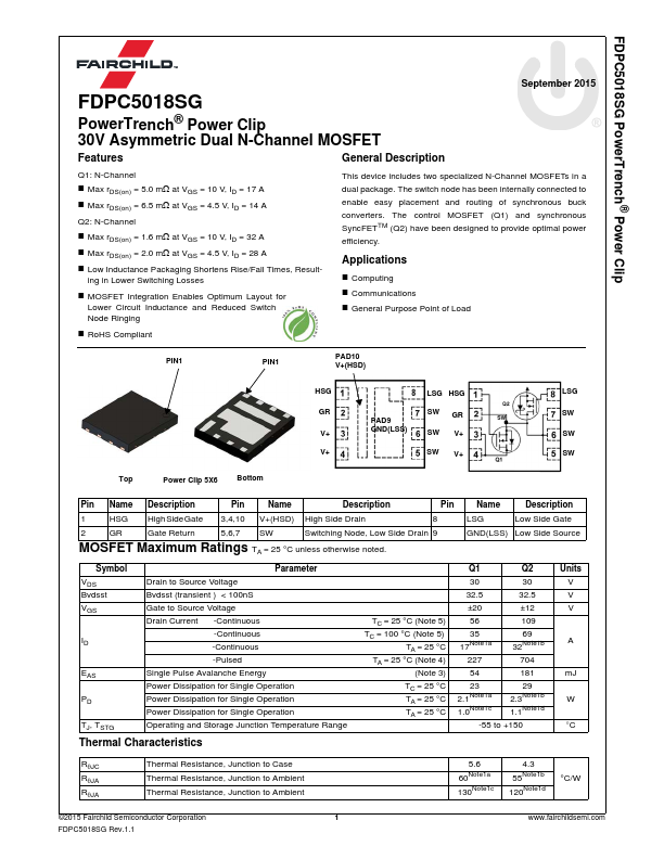
FDPC5018SG PowerTrench® Power Clip
PowerTrench® Power Clip 30V Asymmetric Dual N-Channel MOSFET
September 2015
Features
General Description
Q1: N-Channel
- Max rDS(on) = 5.0 mΩ at VGS = 10 V, ID = 17 A
- Max rDS(on) = 6.5 mΩ at VGS = 4.5 V, ID = 14 A
Q2: N-Channel
- Max rDS(on) = 1.6 mΩ at VGS = 10 V, ID = 32 A
- Max rDS(on) = 2.0 mΩ at VGS = 4.5 V, ID = 28 A
- Low Inductance Packaging Shortens Rise/Fall Times, Result- ing in Lower Switching Losses
- MOSFET Integration Enables Optimum Layout for Lower Circuit Inductance and Reduced Switch Node Ringing
This device includes two specialized N-Channel MOSFETs in a dual package. The switch node has been internally connected to...