FDT86113LZ
Features
General Description
- Max r DS(on) = 100 m: at VGS = 10 V, ID = 3.3 A
- Max r DS(on) = 145 m: at VGS = 4.5 V, ID = 2.7 A
- High performance trench technology for extremely low r DS(on)
- High power and current handling capability in a widely used surface mount package
- HBM ESD protection level > 3 KV typical (Note 4)
- 100% UIL tested
This N-Channel logic Level MOSFETs are produced using Fairchild Semiconductor‘s advanced Power Trench® process that has been special tailored to minimize the on-state resistance and yet maintain superior switching performance. G-S zener has been added to enhance ESD voltage level.
Application
- DC
- DC Switch
- Ro HS pliant
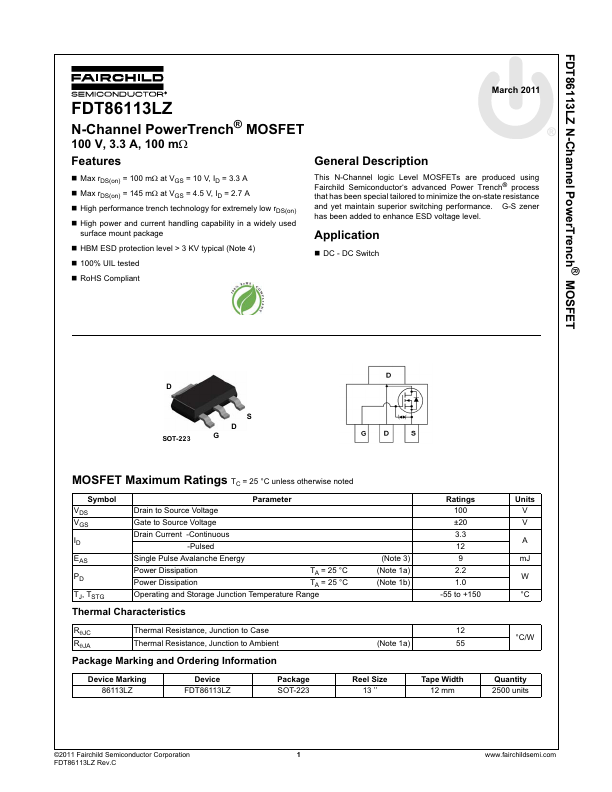
SOT-223
MOSFET Maximum Ratings TC = 25 °C unless otherwise noted
Symbol VDS VGS
TJ, TSTG
Parameter
Drain to Source Voltage
Gate to Source Voltage
Drain Current...