FEATURES
VCE(SAT) = 4.4V at IC=150A tfl = 1.1µs, td(OFF)I = 0.46µs 2kV ESD Protected High Peak Current Density TSSOP - 8 package, small footprint, low profile (1mm thick) GENERAL DESCRIPTION
The gate is ESD protected with a zener diode. APPLICATIONS
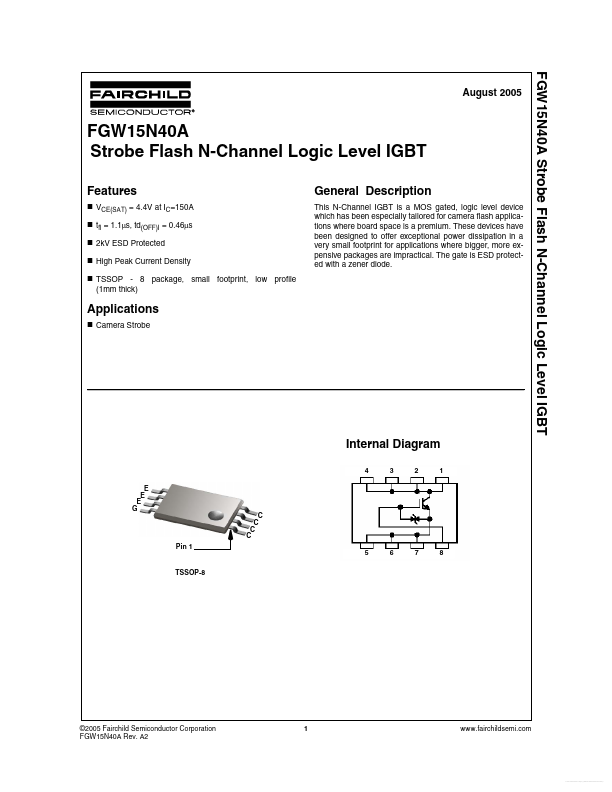
Camera Strobe Internal Diagram 4 E E E G C C C C Pin 1 5 6 7 8 3 2 1 TSSOP-8 ©2005 Fairchild Semiconductor Corporation FGW15N40A Rev. A2 1 Free Datasheet FGW15N40A Strobe Flash N-Channel Logic Level IGBT Device MAXIMUM RATINGS
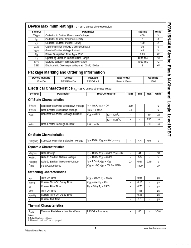
TA = 25°C unless otherwise noted Symbol BVCES IC ICP VGES VGEP PD TJ TSTG ESD Parameter Collector to Emitter Breakdown Voltage Collector Current Continuous(DC) Collector Current Pulsed(100µs) Gate to Emitter Voltage Continuous(DC) Gate to Emitter Voltage Pulsed Power Dissipation Total TC = 25°C Operating Junction Temperature Range Storage Junction Temperature Range Electrostatic Discharge Voltage at 100pF, 1500Ω Ratings 400 8 150 ±6 ±8 1.25 -40 to 150 -40 to 150 2 Units V A A V V W °C °C kV Package Marking... Fairchild Semiconductor