• Part: FIN1048
  • Description: 3.3V LVDS 4-Bit Flow-Through High Speed Differential Receiver
  • Manufacturer: Fairchild Semiconductor
  • Size: 249.78 KB
Download FIN1048 Datasheet PDF
Fairchild Semiconductor
FIN1048
FIN1048 is 3.3V LVDS 4-Bit Flow-Through High Speed Differential Receiver manufactured by Fairchild Semiconductor.
FIN1048 3.3V LVDS 4-Bit Flow-Through High Speed Differential Receiver September 2001 Revised August 2003 FIN1048 3.3V LVDS 4-Bit Flow-Through High Speed Differential Receiver General Description 
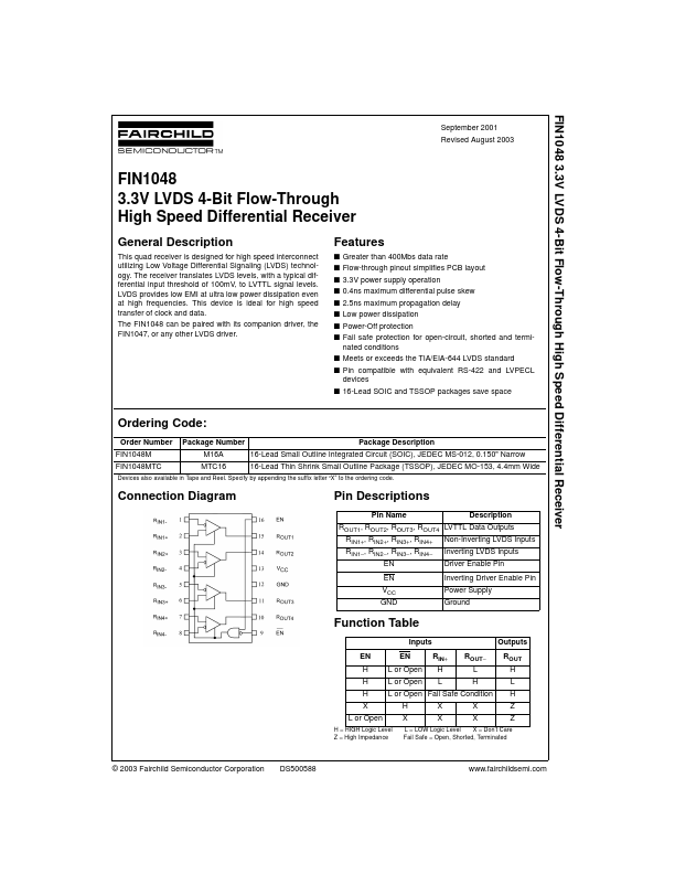
This quad receiver is designed for high speed interconnect utilizing Low Voltage Differential Signaling (LVDS) technology. The receiver translates LVDS levels, with a typical differential input threshold of 100m V, to LVTTL signal levels. LVDS provides low EMI at ultra low power dissipation even at high frequencies. This device is ideal for high speed transfer of clock and data. The FIN1048 can be paired with its panion driver, the FIN1047, or any other LVDS driver. Features s Greater than 400Mbs data rate s Flow-through pinout simplifies PCB layout s 3.3V power supply operation s 0.4ns maximum differential pulse skew s 2.5ns maximum propagation delay s Low power dissipation s Power-Off protection s Fail safe protection for open-circuit, shorted and terminated conditions s Meets or exceeds the TIA/EIA-644 LVDS standard s Pin patible with equivalent RS-422 and LVPECL devices s 16-Lead SOIC and TSSOP packages save space Ordering Code: Order Number FIN1048M FIN1048MTC Package Number M16A MTC16 Package Description 16-Lead Small Outline Integrated Circuit (SOIC), JEDEC MS-012, 0.150" Narrow 16-Lead Thin Shrink Small Outline Package (TSSOP), JEDEC MO-153, 4.4mm Wide Devices also available in Tape and Reel. Specify by appending the suffix letter “X” to the ordering code. Connection Diagram Pin Descriptions Pin Name RIN1+, RIN2+, RIN3+, RIN4+ RIN1- , RIN2- , RIN3- , RIN4- EN EN VCC GND Description Non-Inverting LVDS Inputs Inverting LVDS Inputs Driver Enable Pin Inverting Driver Enable Pin Power Supply Ground ROUT1, ROUT2, ROUT3, ROUT4 LVTTL Data Outputs Function Table Inputs EN H H H X L or Open H = HIGH Logic Level Z = High Impedance Outputs RIN+ H L X X ROUT- L H X X ROUT H L H Z Z EN L or Open L or Open H X L or Open Fail Safe Condition L = LOW Logic Level X =...