FJV3104R
Switching Application (Bias Resistor Built In)
- Switching circuit, Inverter, Interface circuit Driver Circuit,
- Built in bias Resistor (R1=47KΩ, R2=47KΩ)
- plement to FJV4104R
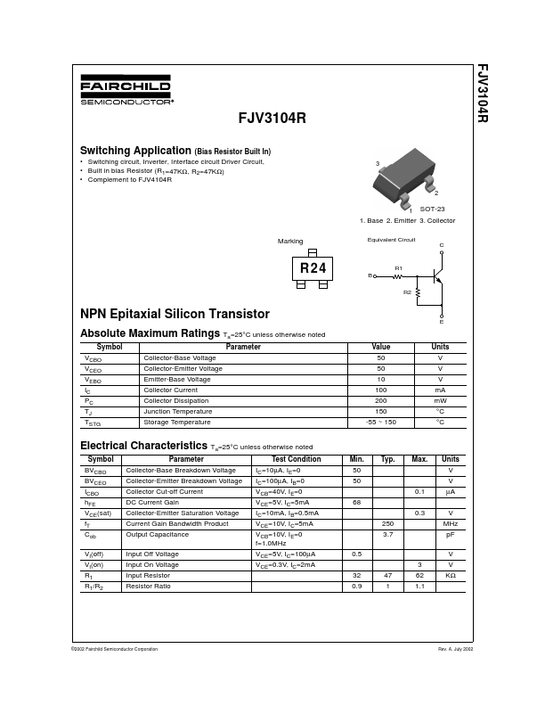
2 1
SOT-23
1. Base 2. Emitter 3. Collector Marking
Equivalent Circuit C
R24
R1 B R2
NPN Epitaxial Silicon Transistor
Absolute Maximum Ratings Ta=25°C unless otherwise noted
Symbol VCBO VCEO VEBO IC PC TJ TSTG Parameter Collector-Base Voltage Collector-Emitter Voltage Emitter-Base Voltage Collector Current Collector Dissipation Junction Temperature Storage Temperature Value 50 50 10 100 200 150 -55 ~ 150
Units V V V m A m W °C °C
Electrical Characteristics Ta=25°C unless otherwise noted
Symbol BVCBO BVCEO ICBO h FE VCE(sat) f T Cob VI(off) VI(on) R1 R1/R2 Parameter Collector-Base Breakdown Voltage Collector-Emitter Breakdown Voltage Collector Cut-off Current DC Current Gain Collector-Emitter Saturation Voltage Current Gain Bandwidth Product Output Capacitance Input Off Voltage Input...