FOD3120
FOD3120 is Gate Drive Optocoupler manufactured by Fairchild Semiconductor.
Features
- High Noise Immunity Characterized by 35 k V/μs Minimum mon Mode Rejection
- 2.5 A Peak Output Current Driving Capability for Most 1200 V/20 A IGBT
- Use of P-channel MOSFETs at Output Stage Enables Output Voltage Swing Close to The Supply Rail
- Wide Supply Voltage Range from 15 V to 30 V
- Fast Switching Speed
- 400 ns max. Propagation Delay
- 100 ns max. Pulse Width Distortion
- Under Voltage Lock Out (UVLO) with Hysteresis
- Extended Industrial Temperate Range, -40°C to 100°C Temperature Range
- Safety and Regulatory Approved
- UL1577, 5000 VRMS for 1 min.
- DIN EN/IEC60747-5-5
- RDS(ON) of 1 Ω (typ.) Offers Lower Power Dissipation
- >8.0 mm Clearance and Creepage Distance (Option ‘T’ or ‘TS’)
- 1,414 V Peak Working Insulation Voltage (VIORM)
Applications
- Industrial Inverter
- Uninterruptible Power Supply
- Induction Heating
- Isolated IGBT/Power MOSFET Gate Drive
Description
The FOD3120 is a 2.5 A Output Current Gate Drive Optocoupler, capable of driving most medium power IGBT/MOSFET. It is ideally suited for fast switching driving of power IGBT and MOSFETs used in motor control inverter applications, and high performance power system.
It utilizes Fairchild’s coplanar packaging technology, Optoplanar®, and optimized IC design to achieve high noise immunity, characterized by high mon mode rejection.
It consists of a gallium aluminum arsenide (Al Ga As) light emitting diode optically coupled to an integrated circuit with a high-speed driver for push-pull MOSFET output stage.
Related Resources
- FOD3150, 1 A Output Current, Gate Drive Optocoupler Datasheet
- .fairchildsemi./products/optoelectronics/
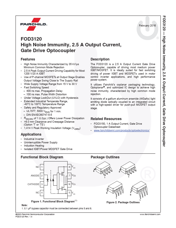
Functional Block Diagram
Package Outlines
NC 1 ANODE 2 CATHODE 3
V DD
7 VO2
6 VO1
NC 4
5V SS
Figure 1. Functional Block Diagram(1)
Note:...