FEATURES
1.2 to 5.5V Input Voltage Range Typical RDS(ON) = 50mΩ @ VIN = 5.5V Typical RDS(ON) = 55mΩ @ VIN = 3.3V ESD Protected, above 2000V HBM tm GENERAL DESCRIPTION
Switch control is by a logic input (ON) capable of interfacing directly with low voltage control signals. Optional on-chip load resistor is added for output quick discharge when switch is turned off. APPLICATIONS
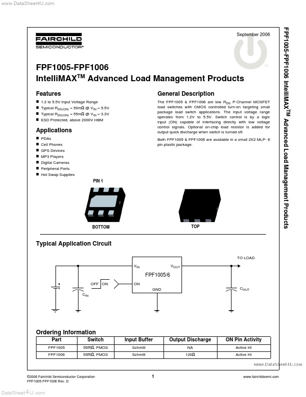
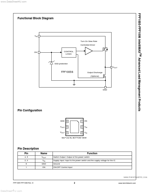
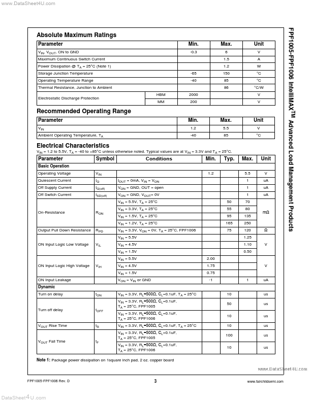
PDAs Cell Phones GPS Devices MP3 Players Digital Cameras Peripheral Ports Hot Swap Supplies PIN 1 BOTTOM TOP Typical Application Circuit TO LOAD VIN VOUT FPF1005/6 OFF ON ON GND CIN COUT - Ordering Information Part FPF1005 FPF1006 Switch 55mΩ, PMOS 55mΩ, PMOS Input Buffer Schmitt Schmitt Output Discharge NA 120Ω ON Pin Activity Active HI Active HI ©2006 Fairchild Semiconductor Corporation FPF1005-FPF1006 Rev. D 1 DataSheet 4 U .com FPF1005-FPF1006 IntelliMAXTM Advanced Load Management Products Functional Block Diagram VIN Turn-On Slew Rate Controlled Driver CONTROL LOGIC ON ESD protection VO... Fairchild Semiconductor