FQB8N90C
Description
These N-Channel enhancement mode power field effect transistors are produced using Fairchild’s proprietary, planar stripe, DMOS technology. This advanced technology has been especially tailored to minimize on-state resistance, provide superior switching performance, and withstand high energy pulse in the avalanche and mutation mode. These devices are well suited for high efficiency switch mode power supplies.
December 2013
Features
- 6.3 A, 900 V, RDS(on) = 1.9 Ω (Max.) @ VGS = 10 V
- Low Gate Charge (Typ. 35 n C)
- Low Crss (Typ. 12 p F)
- Fast Switching
- 100% Avalanche Tested
- Improved dv/dt Capability
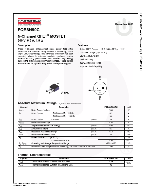
D2-PAK
Absolute Maximum Ratings TC = 25°C unless otherwise noted.
Symbol VDSS ID
IDM VGSS EAS IAR EAR dv/dt PD
TJ, TSTG TL
Parameter
Drain-Source Voltage
Drain Current Drain Current
- Continuous (TC = 25°C)
- Continuous (TC = 100°C)
- Pulsed
(Note 1)
Gate-Source Voltage
Single Pulsed Avalanche Energy
(Note 2)
Avalanche Current
(Note...