ILC5062
ILC5062 is SOT-23 Power Supply reset Monitor manufactured by Fairchild Semiconductor.
Features
- -
- -
- -
- All-CMOS design in SOT-23 or SC70 package A grade ±1% precision in Reset Detection Standard grade : ±2% precision in Reset Detection Only 1µA of Iq Over 2m A of sink current capability Built-in hysteresis of 5% of detection voltage Voltage options of 2.6, 2.7, 2.8, 2.9, 3.1, 4.4, and 4.6V fit most supervisory applications
- Active low push-pull output
Description
All-CMOS voltage monitoring circuit in either a 3-lead SOT-23 or SC70 package offers the best performance in power consumption and accuracy. The ILC5062 is available in a series of ±1% (A-grade) or 2% (standard grade) accurate trip voltages to fit most microprocessor applications. Even though its output can sink over 2m A, the device draws only 1µA in normal operation. Additionally, a built-in hysteresis of 5% of detect voltage simplifies system design.
Applications
- -
- - Microprocessor reset circuits Memory battery back-up circuitry Power-on reset circuits Portable and battery powered electronics
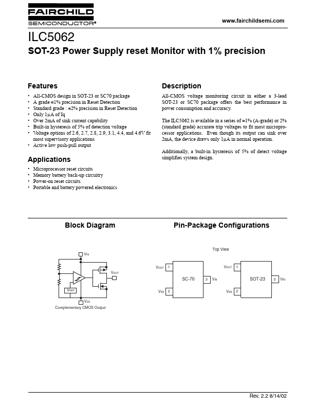
Block Diagram
Pin-Package Configurations
Top View
VOUT
VOUT
VOUT
SC-70
VREF VSS plementary CMOS Output
VIN VSS 2
SOT-23
Rev. 2.2 8/14/02
PRODUCT SPECIFICATION
Absolute Maximum Ratings
Parameter Input Voltage Output Current Output Voltage Continuous Total Power Dissipation (SOT-23) Operating Ambient Temperature Storage Temperature Symbol VIN IOUT VOUT PD Topr Tstg Ratings 12 50 VSS-0.3~VIN=+0.3 150 -30~+80 -40~+125 Units V m A V m W °C °C
Electrical Characterisitcs ILC5062 (TA=25°C)
Parameter Detect Fail Voltage Detect Fail Voltage Hysteresis Range Supply Current Symbol VDF VDF VHYS Conditions A grade Standard grade VIN = 1.5V VIN = 2.0V VIN = 3.0V VIN = 4.0V VIN = 5.0V VDF = 2.1 ~ 6.0V N-ch VDS = 0.5V VIN = 1.0V VIN = 2.0V VIN = 3.0V VIN = 4.0V VIN = 5.0V P-Ch VDS = 2.1V VIN = 8V Temperature Characteristics ∆VDF/(∆Topr- VDF) -30°C < Topr < 80°C Delay Time (Release t DLY Voltage Output Inversion) (VDR to VOUT Inversion) -200 Min. VDF X 0.99...