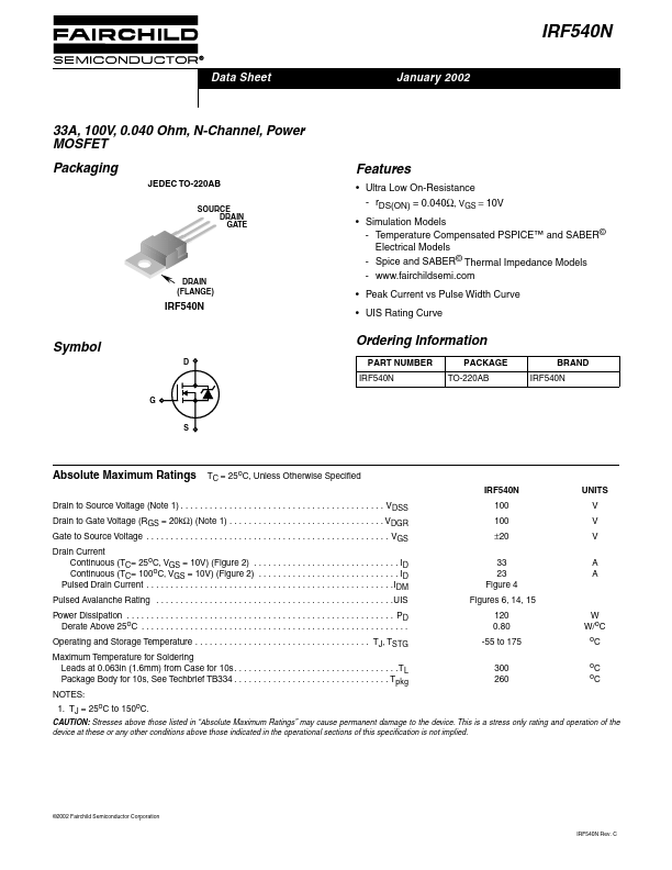
IRF540N
Key Features
- Ultra Low On-Resistance
- rDS(ON) = 0.040Ω, VGS = 10V
- Simulation Models
- Spice and SABER© Thermal Impedance Models
- fairchildsemi
- Peak Current vs Pulse Width Curve
- UIS Rating Curve
| Part Number | Manufacturer | Description |
|---|---|---|
| IRF540NPbF | International Rectifier | Power MOSFET |
| IRF540NLPbF | International Rectifier | Power MOSFET |
| IRF540N | International Rectifier | Power MOSFET |
| IRF540NS | International Rectifier | Power MOSFET |
| IRF540NPBF | Inchange Semiconductor | N-Channel MOSFET |
| IRF540NL | International Rectifier | Power MOSFET |
| IRF540NS | Kexin Semiconductor | N-Channel MOSFET |
| IRF540NSPbF | International Rectifier | Power MOSFET |
| F540NS | International Rectifier | IRF540NS |
| IRF540NL | Inchange Semiconductor | N-Channel MOSFET |