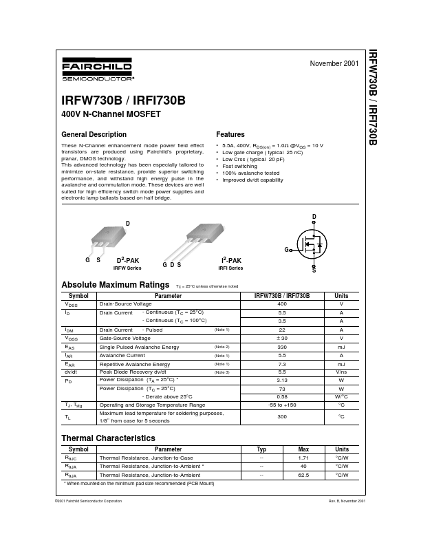
These N-Channel enhancement mode power field effect transistors are produced using Fairchild’s proprietary, planar, DMOS technology.
Key Features
5.5A, 400V, RDS(on) = 1.0Ω @VGS = 10 V Low gate charge ( typical 25 nC) Low Crss ( typical 20 pF) Fast switching 100% avalanche tested Improved dv/dt capability
D D
!.
◀
▲.
G! G S
D2-PAK
IRFW Series
G D S
I2-PAK
IRFI Series
!
S
Absolute Maximum Ratings
Symbol VDSS ID IDM VGSS EAS IAR EAR dv/dt PD
TC = 25°C unless otherwise noted
Parameter Drain-Source Voltage - Continuous (TC = 25°C) Drain Current - Continuou.
Full PDF Text Transcription for IRFI730B (Reference)
Note: Below is a high-fidelity text extraction (approx. 800 characters) for
IRFI730B. For precise diagrams, and layout, please refer to the original PDF.
IRFW730B / IRFI730B November 2001 IRFW730B / IRFI730B 400V N-Channel MOSFET General Description These N-Channel enhancement mode power field effect transistors are produc...
View more extracted text
e N-Channel enhancement mode power field effect transistors are produced using Fairchild’s proprietary, planar, DMOS technology. This advanced technology has been especially tailored to minimize on-state resistance, provide superior switching performance, and withstand high energy pulse in the avalanche and commutation mode. These devices are well suited for high efficiency switch mode power supplies and electronic lamp ballasts based on half bridge. Features • • • • • • 5.5A, 400V, RDS(on) = 1.