Fairchild Semiconductor J109
N-Channel Switch
| Part No. | J109 |
|---|---|
| Datasheet | J109 Download |
| Manufacturer |  Fairchild Semiconductor |
| Description | N-Channel Switch |
| Buy | Stock & Price |
FEATURES
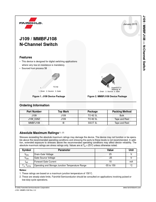
● This device is designed for digital switching applications where very low on resistance is mandatory.● Sourced from process 58 1 TO-92 1. Drain 2. Source 3. Gate Figure 1. J109 Device Package Ordering Information Part Number J109 J109_D26Z MMBFJ108 Top Mark J109 J109 I8 3 2 1 SuperSOT-3 Marking: I8 1. Drain 2. Source 3. Gate Figure 2. MMBFJ108 Device Package Package TO-92 3L TO-92 3L SSOT 3L Packing Method Bulk Tape and Reel Tape and Reel
ABSOLUTE MAXIMUM RATINGS
(1), (2) Stresses exceeding the absolute maximum ratings may damage the device. The device may not function or be operable above the recommended operating conditions and stressing the parts to these levels is not recommended. In addition, extended exposure to stresses above the recommended operating conditions may affect device reliability. The absolute maximum ratings are stress ratings only. Values are at TA = 25°C unless otherwise noted. Symbol Parameter Value Unit VDG VGS IGF TJ, TSTG Drain-Gate Voltage Gate-Source Voltage Forward Gate Current Operating and Storage Junction Temperature Range 25 -25 10 -55 to 150 V V mA °C Notes: 1.
