Datasheet4U.com
🌙
JFTJ105 Datasheet | Fairchild Semiconductor
Part:
JFTJ105
Description:
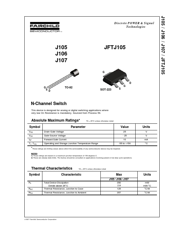
N-Channel Switch
Manufacturer:
Fairchild Semiconductor
Size:
61.02 KB
JFTJ105 Datasheet (PDF) Download
Fairchild Semiconductor
JFTJ105
Key Features
These ratings are limiting values above which the serviceability of any semiconductor device may be impaired
4.5 - 2.0 - 0.5
×
Close