Fairchild Semiconductor KA224A
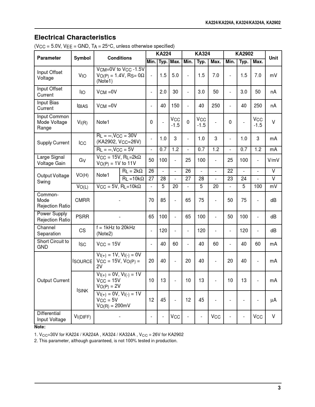
the KA224; and the 0°C ≤ TA ≤ +70°C for the KA324 ; and the -40°C ≤ TA ≤ +85°C for the KA2902 Parameter Input Offset Voltage Input Offset Voltage Drift Input Offset Current Input Offset Current Drift Input Bias Current Input Common Mode Voltage Range Large Signal Voltage Gain Output Voltage Swing Symbol Conditions VICM = 0V to VCC -1.5V VO(P) = 1.4V, RS = 0Ω (Note1) RS = 0Ω (Note2) VCM = 0V RS = 0Ω (Note2) VCM = 0V Note1 VCC = 15V, RL = 2.0kΩ VO(P) = 1V to 11V Note1 RL = 2kΩ RL = 10kΩ KA224 KA324 KA2902 Unit Min.| Part No. | KA224A |
|---|---|
| Datasheet | KA224A Download |
| Manufacturer |  Fairchild Semiconductor |
| Description | Quad Operational Amplifier |
| Buy | Stock & Price |
FEATURES
● Internally Frequency Compensated for Unity Gain● Large DC Voltage Gain: 100dB
● Wide Power Supply Range: KA224 / KA224A, KA324 / KA324A : 3V~32V (or ±1.5 ~ 16V) KA2902: 3V~26V (or ±1.5V ~ 13V)
● Input Common Mode Voltage Range Includes Ground
● Large Output Voltage Swing: 0V to VCC -1.5V
● Power Drain Suitable for Battery Operation
DESCRIPTION
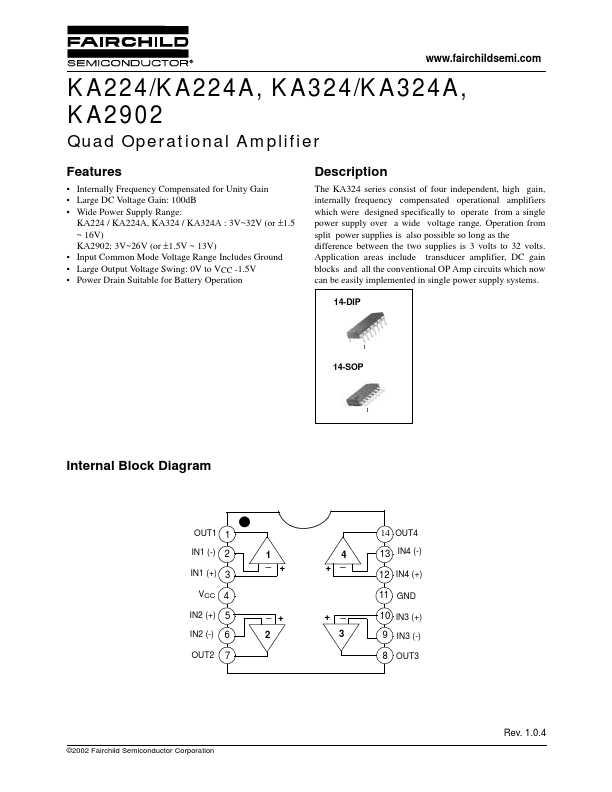
The KA324 series consist of four independent, high gain, internally frequency compensated operational amplifiers which were designed specifically to operate from a single power supply over a wide voltage range. Operation from split power supplies is also possible so long as the difference between the two supplies is 3 volts to 32 volts. Application areas include transducer amplifier, DC gain blocks and all the conventional OP Amp circuits which now can be easily implemented in single power supply systems. 14-DIP 1 14-SOP 1 Internal Block Diagram OUT1 1 IN1 (-) 14 OUT4 1 _ + 4 _ 13 IN4 (-) 12 IN4 (+) 11 GND _ + 2 + _ 3 10 IN3 (+) 9 IN3 (-) 8 OUT3 2 IN1 (+) 3 VCC 4 IN2 (+) IN2 (-) OUT2 + 5 6 7 Rev.