GENERAL DESCRIPTION
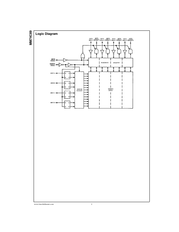
Inputs to the memory consist of four address lines, four data input lines, a write enable line and a memory enable line. An internal address register latches the address information on the positive to negative transition of the memory enable input. Address Operation: Address inputs must be stable tSA prior to the positive to negative transition of memory enable. It is thus not necessary to hold address information stable for more than tHA after the memory is enabled (positive to negative transition of memory enable). Write Operation: Information present at the data inputs is written into the memory at the selected address by bringing write enable and memory enable LOW. Read Operation: The complement of the information which was written into the memory is non-destructively read out at the four outputs. This is accomplished by selecting the desired address and bringing memory enable LOW and write enable HIGH. When the device is writing or disabled the output assumes a 3-STATE (Hi-z) condition. Fairchild Semiconductor