MOCD223-M
DESCRIPTION
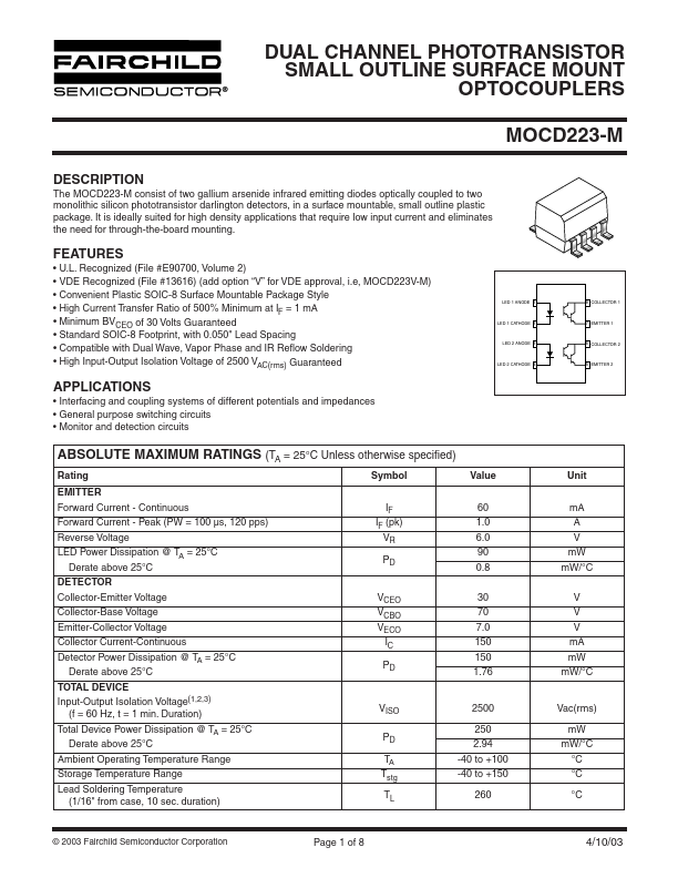
The MOCD223-M consist of two gallium arsenide infrared emitting diodes optically coupled to two monolithic silicon phototransistor darlington detectors, in a surface mountable, small outline plastic package. It is ideally suited for high density applications that require low input current and eliminates the need for through-the-board mounting.
FEATURES
- U.L. Recognized (File #E90700, Volume 2)
- VDE Recognized (File #13616) (add option “V” for VDE approval, i.e, MOCD223V-M)
- Convenient Plastic SOIC-8 Surface Mountable Package Style
- High Current Transfer Ratio of 500% Minimum at IF = 1 m A
- Minimum BVCEO of 30 Volts Guaranteed
- Standard SOIC-8 Footprint, with 0.050" Lead Spacing
- patible with Dual Wave, Vapor Phase and IR Reflow Soldering
- High Input-Output Isolation Voltage of 2500 VAC(rms) Guaranteed
LED 1 ANODE 1
8 COLLECTOR 1
LED 1 CATHODE 2
7 EMITTER 1
LED 2 ANODE 3
6 COLLECTOR 2
LED 2 CATHODE 4
5 EMITTER 2
APPLICATIONS
- Interfacing and coupling...