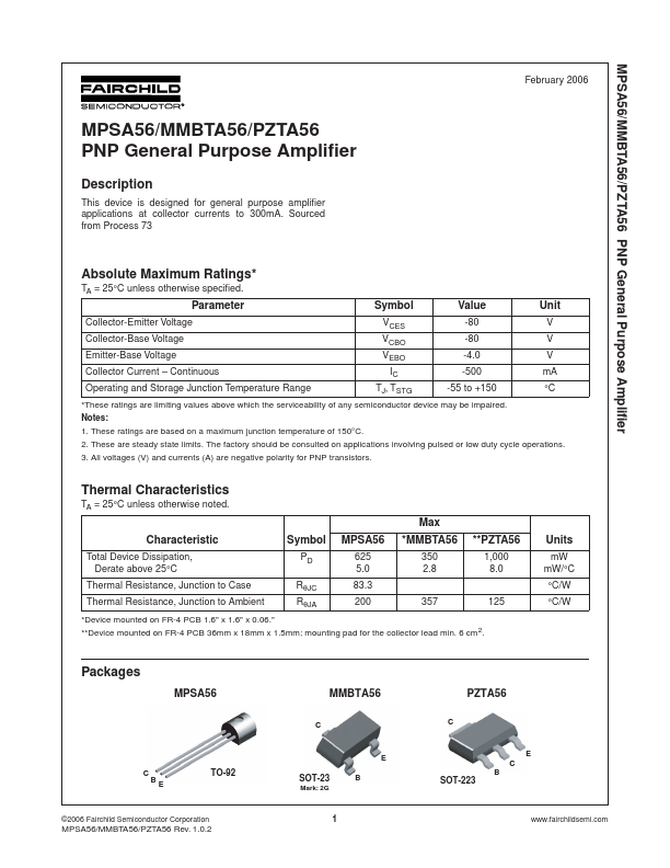
MPSA56
Description
This device is designed for general purpose amplifier applications at collector currents to 300m A. Sourced from Process 73
Absolute Maximum Ratings-
TA = 25°C unless otherwise specified.
Parameter
Symbol
Value
Unit
Collector-Emitter Voltage
VCES
-80
Collector-Base Voltage
VCBO
-80
Emitter-Base Voltage
VEBO
-4.0
Collector Current
- Continuous
-500 m A
Operating and Storage Junction Temperature Range
TJ, TSTG
-55 to +150
°C
- These ratings are limiting values above which the serviceability of any semiconductor device may be impaired.
Notes:
1. These ratings are based on a maximum junction temperature of 150°C.
2. These are steady state limits. The factory should be consulted on applications involving pulsed or low duty cycle operations.
3. All voltages (V) and currents (A) are negative polarity for PNP transistors.
Thermal Characteristics
TA = 25°C unless otherwise noted.
Max
Characteristic
Symbol MPSA56
- MMBTA56
- -...