Fairchild Semiconductor N316AD
This device employs a new advanced trench MOSFET technology and features low gate charge while maintaining low on-resistance. Optimized for switching applications, this device improves the overall efficiency of DC/DC converters and allows operation to higher switching frequencies.| Part No. | N316AD |
|---|---|
| Datasheet | N316AD Download |
| Manufacturer |  Fairchild Semiconductor |
| Description | N-channel Logic Level PWM Optimized Ultrafet Trench Power Mosfets |
| Buy | Stock & Price |
GENERAL DESCRIPTION
FEATURES
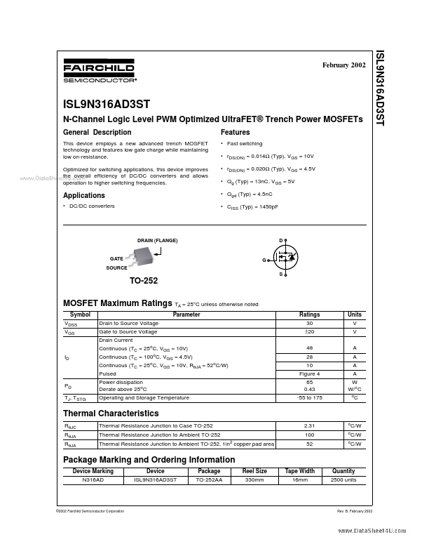
● Fast switching● rDS(ON) = 0.014Ω (Typ), VGS = 10V
● rDS(ON) = 0.020Ω (Typ), VGS = 4.5V
● Qg (Typ) = 13nC, VGS = 5V
● Qgd (Typ) = 4.5nC
● CISS (Typ) = 1450pF
APPLICATIONS
● DC/DC converters DRAIN (FLANGE) D GATE SOURCE G S TO-252 MOSFETMAXIMUM RATINGS
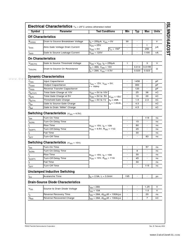
TA = 25°C unless otherwise noted Symbol VDSS VGS Parameter Drain to Source Voltage Gate to Source Voltage Drain Current Continuous (TC = 25oC, VGS = 10V) ID Continuous (TC = 100oC, VGS = 4.5V) Continuous (TC = 25oC, VGS = 10V, RθJA = 52oC/W) Pulsed PD TJ, TSTG Power dissipation Derate above 25oC Operating and Storage Temperature 48 28 10 Figure 4 65 0.43 -55 to 175 A A A A W W/oC o Ratings 30 ±20 Units V V C Thermal Characteristics RθJC RθJA RθJA Thermal Resistance Junction to Case TO-252 Thermal Resistance Junction to Ambient TO-252 Thermal Resistance Junction to Ambient TO-252, 1in2 copper pad area 2.31 100 52 o C/W C/W oC/W o Package Marking and Ordering Information Device Marking N316AD Device ISL9N316AD3ST Package TO-252AA Reel Size 330mm Tape Width 16mm Quantity 2500 units ©2002 Fairchild Semiconductor Corporation Rev.