The following content is an automatically extracted verbatim text
from the original manufacturer datasheet and is provided for reference purposes only.
View original datasheet text
PF5103 N-Channel Switch
October 2006
PF5103
N-Channel Switch
Features
• This device is designed for low level analog switching sample and hold circuits and chopper stabilized amplifiers. • 
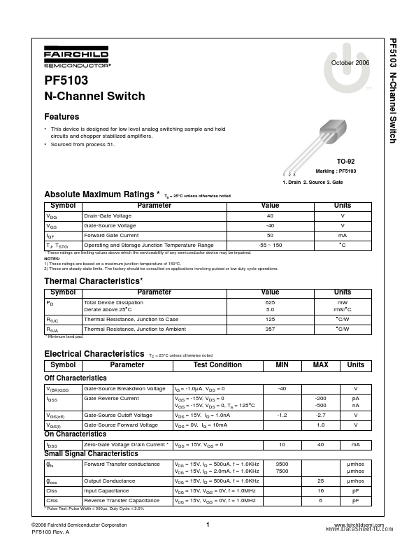
Sourced from process 51.
tm
TO-92
1 2 3
Marking : PF5103
1. Drain 2. Source 3. Gate
Absolute Maximum Ratings *
Symbol
VDG VGS IGF TJ, TSTG Drain-Gate Voltage Gate-Source Voltage Forward Gate Current
Ta = 25°C unless otherwise noted
Parameter
Value
40 -40 50 -55 ~ 150
Units
V V mA °C
Operating and Storage Junction Temperature Range
* These ratings are limiting values above which the serviceability of any semiconductor device may be impaired. NOTES: 1) These ratings are based on a maximum junction temperature of 150°C. 2) These are steady state limits.