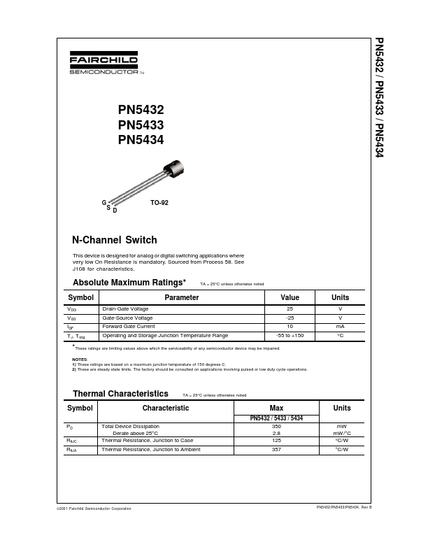
PN5433 Overview
| Part | PN5433 |
|---|---|
| Description | N-Channel Switch |
| Manufacturer | Fairchild Semiconductor |
| Size | 300.70 KB |
| Seller | Inventory | Price Breaks | Buy |
|---|---|---|---|
| Onlinecomponents.com | 0 | 1+ : 219.14 USD 3+ : 215.85 USD 5+ : 212.61 USD 10+ : 209.42 USD |
View Offer |
| Master Electronics | 0 | 1+ : 219.14 USD 3+ : 215.85 USD 5+ : 212.61 USD 10+ : 209.42 USD |
View Offer |
| Part Number | Manufacturer | Description |
|---|---|---|
| SW-331 | Tyco Electronics | Matched GaAs SPDT Switch |
| B3045G | onsemi | Switch-mode Power Rectifiers |
| DK1203 | Dongke Semiconductor | AC-DC Switch Mode Power controller |