Fairchild Semiconductor RF1S30P06SM
P-Channel Power MOSFET
| Part No. | RF1S30P06SM |
|---|---|
| Datasheet | RF1S30P06SM Download |
| Manufacturer |  Fairchild Semiconductor |
| Description | P-Channel Power MOSFET |
| Buy | Stock & Price |

FEATURES
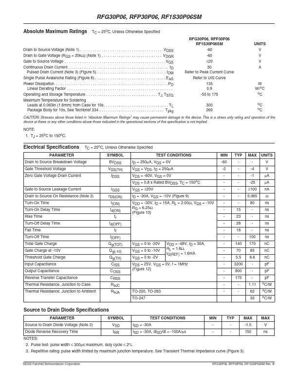
● 30A, 60V● rDS(ON) = 0.065Ω
● Temperature Compensating PSPICE® Model
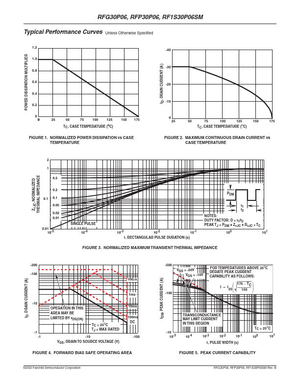
● Peak Current vs Pulse Width Curve
● UIS Rating Curve
● 175oC Operating Temperature
● Related Literature - TB334 “Guidelines for Soldering Surface Mount Components to PC Boards” Symbol D G S JEDEC TO-220AB DRAIN (FLANGE) SOURCE DRAIN GATE JEDEC TO-263AB GATE SOURCE DRAIN (FLANGE) ©2002 Fairchild Semiconductor Corporation RFG30P06, RFP30P06, RF1S30P06SM Rev. B RFG30P06, RFP30P06, RF1S30P06SM
ABSOLUTE MAXIMUM RATINGS
TC = 25oC, Unless Otherwise Specified Drain to Source Voltage (Note 1) . . . . . . . . . . . . . . . . . . . . . . . . . . . . . . . . . . . . . . .VDSS Drain to Gate Voltage (RGS = 20kΩ) (Note 1) . . . . . . . . . . . . . . . . . . . . . . . . . . . . VDGR Gate to Source Voltage . . . . . . . . . . . . . . . . . . . . . . . . . . . . . . . . . . . . . . . . . . . . . . .VGS Continuous Drain Current . . . . . . . . . . . . . . . . . . . . . . . . . . . . . . . . . . . . . . . . . . . . . . ID Pulsed Drain Current (Note 3) (Figure 5) . . . . . . . . . . . . . . . . . . . . . . . . . . . . . . . .