SSD2007A Overview
Key Specifications
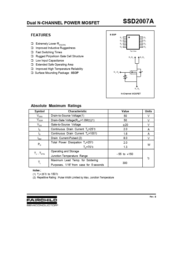
Package: SOIC
Mount Type: Surface Mount
Pins: 8
Max Operating Temp: 150 °C
Key Features
- 1.0 μA VGS=20V
- 1.0 μA VGS=-20V
| Part | SSD2007A |
|---|---|
| Description | Dual N-CHANNEL POWER MOSFET |
| Category | MOSFET |
| Manufacturer | Fairchild Semiconductor |
| Size | 233.88 KB |
Package: SOIC
Mount Type: Surface Mount
Pins: 8
Max Operating Temp: 150 °C
| Seller | Inventory | Price Breaks | Buy |
|---|---|---|---|
| Verical | 15153 | 446+ : 0.8421 USD 500+ : 0.7579 USD 1000+ : 0.699 USD 10000+ : 0.6231 USD |
View Offer |
| Verical | 22434 | 446+ : 0.8421 USD 500+ : 0.7579 USD 1000+ : 0.699 USD 10000+ : 0.6231 USD |
View Offer |
| Part Number | Manufacturer | Description |
|---|---|---|
| SSD2005 | VBsemi | Dual P-Channel 30V MOSFET |