MM74HC259
Description
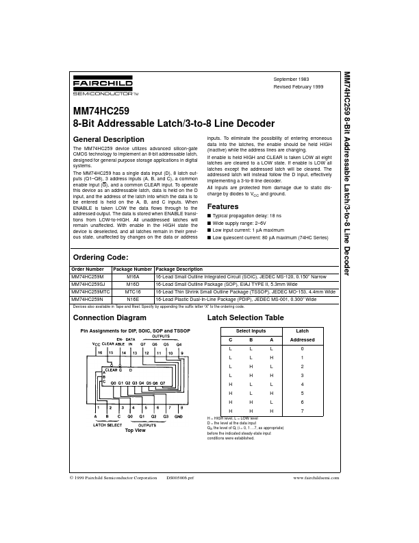
The MM74HC259 device utilizes advanced silicon-gate CMOS technology to implement an 8-bit addressable latch, designed for general purpose storage applications in digital systems.
Key Features
- Specify by appending the suffix letter “X” to the ordering code
- 7, as appropriate) before the indicated steady-state input conditions were established
- © 1999 Fairchild Semiconductor Corporation DS005006.prf .fairchildsemi