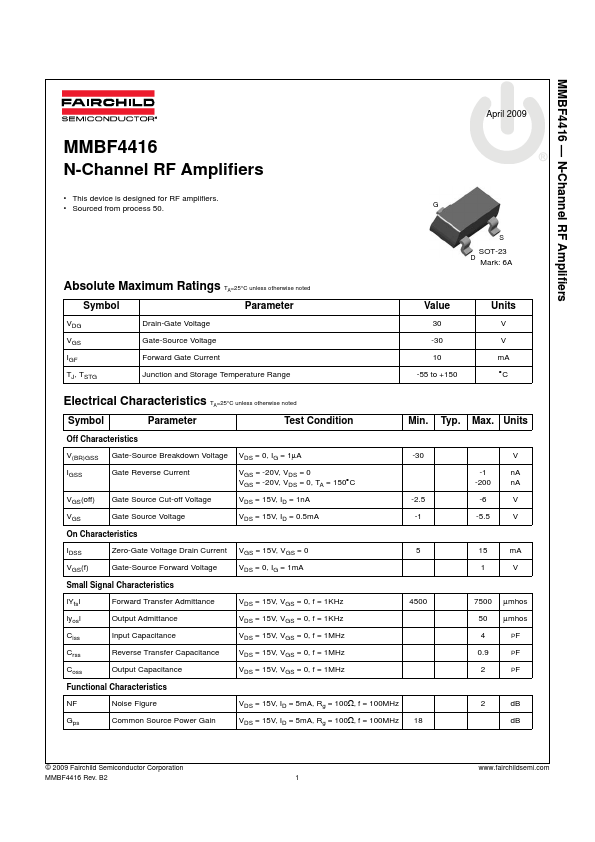
MMBF4416 Overview
Key Features
- This device is designed for RF amplifiers
- Sourced from process 50
| Part | MMBF4416 |
|---|---|
| Description | N-Channel RF Amplifiers |
| Manufacturer | Fairchild Semiconductor |
| Size | 113.47 KB |
| Part Number | Manufacturer | Description |
|---|---|---|
| MMBF4416 | onsemi | N-Channel RF Amplifiers |
| MMBF4416A | onsemi | N-Channel RF Amplifier |
| MMBF4416LT1 | Motorola Semiconductor | JFET VHF/UHF Amplifier Transistor |
| MMBF4416LT1 | onsemi | JFET VHF/UHF Amplifier Transistor |