MMBFJ176
Overview
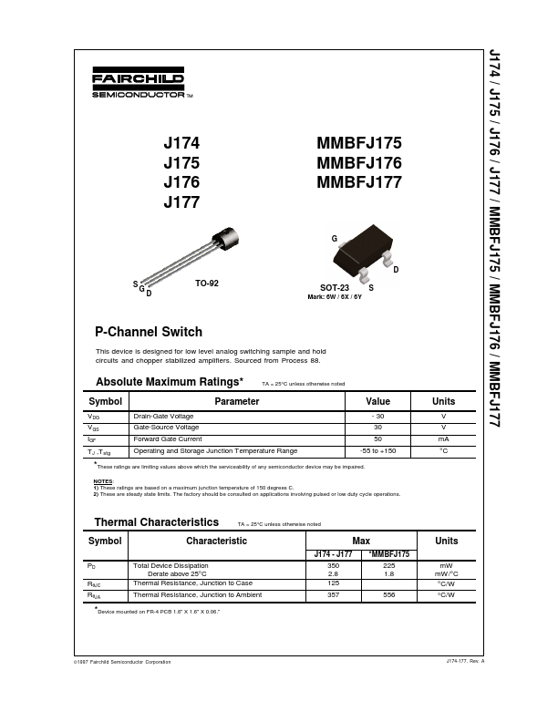
J174 / J175 / J176 / J177 / MMBFJ175 / MMBFJ176 / MMBFJ177 J174 J175 J176 J177 MMBFJ175 MMBFJ176 MMBFJ177 G D S G TO-92 D SOT-23 Mark: 6W / 6X / 6Y S P-Channel Switch This device is designed f...
| Part | MMBFJ176 |
|---|---|
| Description | P-Channel Switch |
| Manufacturer | Fairchild Semiconductor |
| Size | 58.40 KB |
J174 / J175 / J176 / J177 / MMBFJ175 / MMBFJ176 / MMBFJ177 J174 J175 J176 J177 MMBFJ175 MMBFJ176 MMBFJ177 G D S G TO-92 D SOT-23 Mark: 6W / 6X / 6Y S P-Channel Switch This device is designed f...
| Part Number | Manufacturer | Description |
|---|---|---|
| MMBFJ176 | onsemi | P-Channel Switch |
| MMBFJ175 | onsemi | P-Channel Switch |
| MMBFJ175LT1G | onsemi | JFET Chopper |
| MMBFJ177LT1 | onsemi | JFET Chopper |
| MMBFJ177 | onsemi | P-Channel Switch |