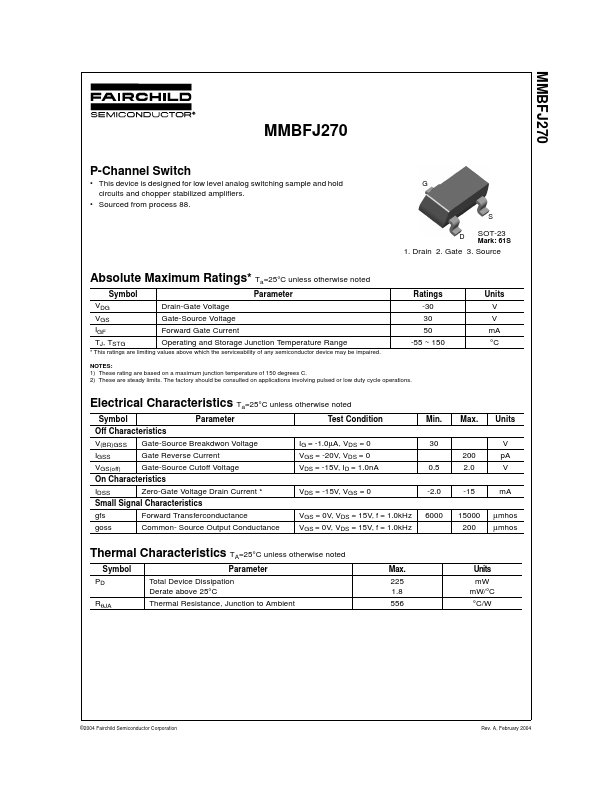
MMBFJ270 Overview
Key Features
- This device is designed for low level analog switching sample and hold circuits and chopper stabilized amplifiers
- Sourced from process 88
| Part | MMBFJ270 |
|---|---|
| Description | P-Channel Switch |
| Manufacturer | Fairchild Semiconductor |
| Size | 46.47 KB |
| Part Number | Manufacturer | Description |
|---|---|---|
| MMBFJ270 | onsemi | P-Channel Switch |