MPSW3725
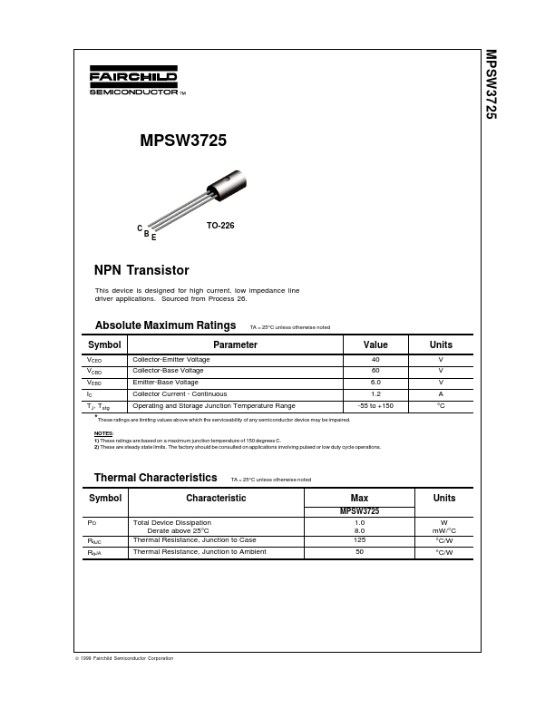
TO-226
NPN Transistor
This device is designed for high current, low impedance line driver applications. Sourced from Process 26.
Absolute Maximum Ratings
Symbol
VCEO VCBO VEBO IC TJ, Tstg Collector-Emitter Voltage Collector-Base Voltage Emitter-Base Voltage Collector Current
- Continuous
TA = 25°C unless otherwise noted
Parameter
Value
40 60 6.0 1.2 -55 to +150
Units
V V V A °C
Operating and Storage Junction Temperature Range
- These ratings are limiting values above which the serviceability of any semiconductor device may be impaired.
NOTES: 1) These ratings are based on a maximum junction temperature of 150 degrees C. 2) These are steady state limits. The factory should be consulted on applications involving pulsed or low duty cycle operations.
Thermal Characteristics
Symbol
PD RθJC RθJA
TA = 25°C unless otherwise noted
Characteristic
Total Device Dissipation Derate above 25°C Thermal Resistance, Junction to Case Thermal Resistance, Junction to...