NDP508AE
NDP508AE is N-Channel Enhancement Mode Field Effect Transistor manufactured by Fairchild Semiconductor.
Description
These N-channel enhancement mode power field effect transistors are produced using Fairchild's proprietary, high cell density, DMOS technology. This very high density process has been especially tailored to minimize on-state resistance, provide superior switching performance, and withstand high energy pulses in the avalanche and mutation modes. These devices are particularly suited for low voltage applications such as automotive, DC/DC converters, PWM motor controls, and other battery powered circuits where fast switching, low in-line power loss, and resistance to transients are needed.
Features
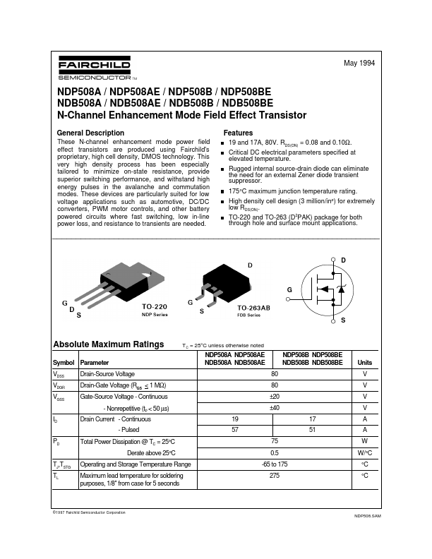
19 and 17A, 80V. RDS(ON) = 0.08 and 0.10Ω. Critical DC electrical parameters specified at elevated temperature. Rugged internal source-drain diode can eliminate the need for an external Zener diode transient suppressor. 175°C maximum junction temperature rating. High density cell design (3 million/in²) for extremely low RDS(ON). TO-220 and TO-263 (D2PAK) package for both through hole and surface mount applications.
Absolute Maximum Ratings
Symbol Parameter VDSS VDGR VGSS ID PD Drain-Source Voltage Drain-Gate Voltage (RGS < 1 MΩ) Gate-Source Voltage
- Continuous
- Nonrepetitive (t P < 50 µs) Drain Current
- Continuous
- Pulsed Total Power Dissipation @ TC = 25°C Derate above 25°C TJ,TSTG TL
TC = 25°C unless otherwise noted
NDP508A NDP508AE NDB508A NDB508AE 80 80 ±20 ±40 19 57 75 0.5
NDP508B NDP508BE NDB508B NDB508BE
Units V V V V
17 51
A A W W/°C °C °C
Operating and Storage Temperature Range Maximum lead temperature for soldering purposes, 1/8" from case for 5 seconds
-65 to 175 275
© 1997 Fairchild Semiconductor Corporation
NDP508.SAM
Electrical Characteristics (T
Symbol EAS IAR Parameter Single Pulse Drain-Source Avalanche Energy
= 25°C unless otherwise noted)
Conditions VDD = 25 V, ID = 19 A
Type NDP508AE NDP508BE NDB508AE NDB508BE
Min
Typ
Max 55 19
Units m J...