FPDA200V
FEATURES
- 21 d Bm Output Power at 1-d B pression at 18 GHz
- 12.5 d B Power Gain at 18 GHz
- 55% Power-Added Efficiency
- Source Vias to Backside Metallization
HIGH PERFORMANCE PHEMT WITH SOURCE VIAS
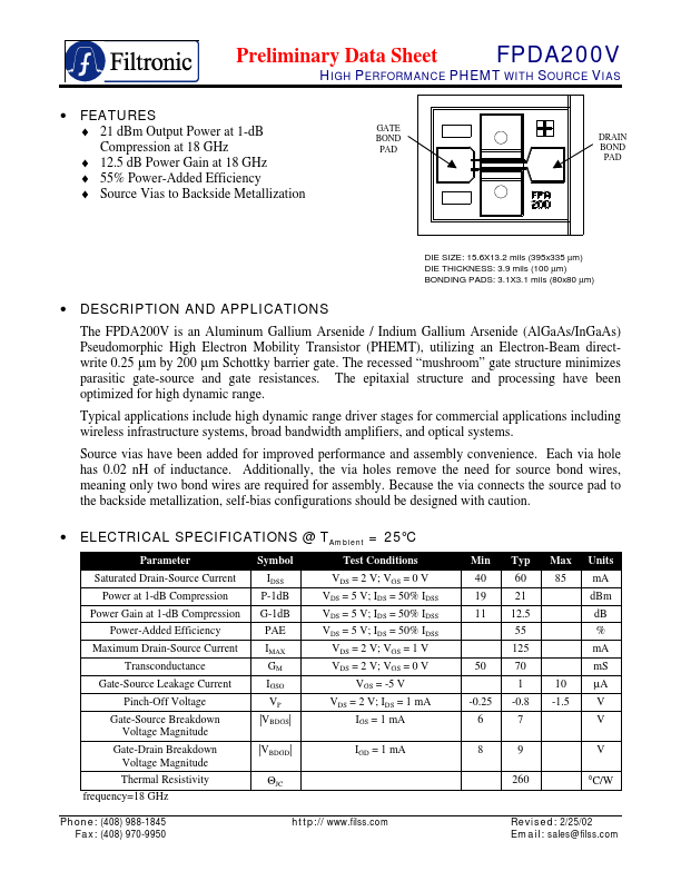
GATE BOND PAD
DRAIN BOND PAD
DIE SIZE: 15.6X13.2 mils (395x335 µm) DIE THICKNESS: 3.9 mils (100 µm) BONDING PADS: 3.1X3.1 mils (80x80 µm)
- DESCRIPTION
AND APPLICATIONS The FPDA200V is an Aluminum Gallium Arsenide / Indium Gallium Arsenide (Al Ga As/In Ga As) Pseudomorphic High Electron Mobility Transistor (PHEMT), utilizing an Electron-Beam directwrite 0.25 µm by 200 µm Schottky barrier gate. The recessed “mushroom” gate structure minimizes parasitic gate-source and gate resistances. The epitaxial structure and processing have been optimized for high dynamic range. Typical applications include high dynamic range driver stages for mercial applications including wireless infrastructure systems, broad bandwidth amplifiers, and optical systems. Source vias have been added for...