Datasheet4U Logo Datasheet4U.com

T25S80A - 8M-BIT SPI NOR FLASH

This page provides the datasheet information for the T25S80A, a member of the T25S80A-First 8M-BIT SPI NOR FLASH family.

Datasheet Summary

Description

4 2.

2.1 Input/Output Summary 6 2.2 Chip Select (/CS) 6 2.3 Serial Clock (SCLK) 6 2.4 Serial Input (SI)/IO0 7 2.5 Serial Data Output (SO)/IO1 7 2.6 Write Protect (/WP)/IO2 7 2.7 HOLD (/HOLD)/IO3 7 2.8 VCC Power Supply 8 2.9 VSS Ground 8 3.

Block/Sector Addresses9 4.

Features

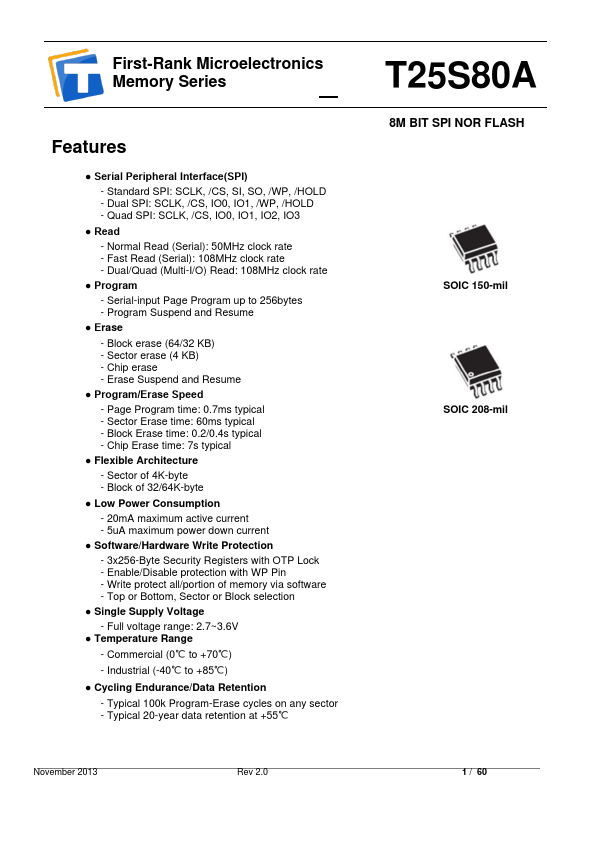
  • Serial Peripheral Interface(SPI) - Standard SPI: SCLK, /CS, SI, SO, /WP, /HOLD - Dual SPI: SCLK, /CS, IO0, IO1, /WP, /HOLD - Quad SPI: SCLK, /CS, IO0, IO1, IO2, IO3.
  • Read - Normal Read (Serial): 50MHz clock rate - Fast Read (Serial): 108MHz clock rate - Dual/Quad (Multi-I/O) Read: 108MHz clock rate.
  • Program - Serial-input Page Program up to 256bytes - Program Suspend and Resume.
  • Erase - Block erase (64/32 KB) - Sector erase (4 KB) - Chip erase - Erase Suspend and Resume.

📥 Download Datasheet

Datasheet preview – T25S80A

Datasheet Details

Part number T25S80A
Manufacturer First-Rank Technology
File Size 2.59 MB
Description 8M-BIT SPI NOR FLASH
Datasheet download datasheet T25S80A Datasheet
Additional preview pages of the T25S80A datasheet.
Other Datasheets by First-Rank Technology

Full PDF Text Transcription

Click to expand full text
First-Rank Microelectronics Memory Series Features ● Serial Peripheral Interface(SPI) - Standard SPI: SCLK, /CS, SI, SO, /WP, /HOLD - Dual SPI: SCLK, /CS, IO0, IO1, /WP, /HOLD - Quad SPI: SCLK, /CS, IO0, IO1, IO2, IO3 ● Read - Normal Read (Serial): 50MHz clock rate - Fast Read (Serial): 108MHz clock rate - Dual/Quad (Multi-I/O) Read: 108MHz clock rate ● Program - Serial-input Page Program up to 256bytes - Program Suspend and Resume ● Erase - Block erase (64/32 KB) - Sector erase (4 KB) - Chip erase - Erase Suspend and Resume ● Program/Erase Speed - Page Program time: 0.7ms typical - Sector Erase time: 60ms typical - Block Erase time: 0.2/0.
Published: |