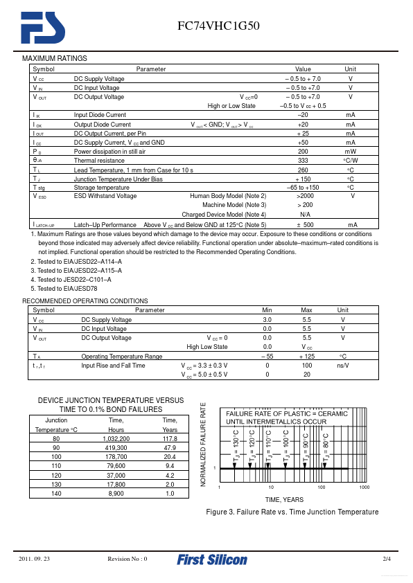
MAXIMUM RATINGS
Symbol V CC V IN V OUT I IK I OK I OUT I CC PD θ JA TL TJ T stg V ESD DC Supply Voltage DC Input Voltage DC Output Voltage Input Diode Current Output Diode Current DC Output Current, per Pin DC Supply Current, V CC and GND Power dissipation in still air Thermal resistance Lead Temperature, 1 mm from Case for 10 s Junction Temperature Under Bias Storage temperature ESD Withstand Voltage V OUT < GND; V OUT > V CC V CC=0 High or Low State Parameter Value – 0.5 to + 7.0 – 0.5 to +7.0 – 0.5 to +7.0 –0.5 to V cc + 0.5 –20 +20 + 25 +50 200 333 260 + 150 –65 to +150 >2000 > 200 N/A Unit V V V mA mA mA mA mW °C/W °C °C °C V Human Body Model (Note 2) Machine Model (Note 3) Charged Device Model (Note 4) Latch–Up Performance Above V CC and Below GND at 125°C (Note 5) ± 500 mA 1. MAXIMUM RATINGS
are those values beyond which damage to the device may occur. Exposure to these conditions or conditions beyond those indicated may adversely affect device reliability. Functional operation under absolute–maximum–rated conditions is not implied. First Silicon