33899
33899 is Programmable H-Bridge Power IC manufactured by Freescale Semiconductor.
Features
- Drives Inductive Loads in a Full H-Bridge Configuration VW SUFFIX (Pb-FREE)
- Current Mirror Output Signal (Gain Selectable via External 98ASH70693A Resistor) 30-PIN HSOP
- Short Circuit Current Limiting
- Thermal Shutdown (Outputs Latched Off Until Reset via SPI) ORDERING INFORMATION
- Internal Charge Pump Circuit for the Internal High-Side MOSFETs Temperature
- SPI-Selectable Slew Rate Control and Current Limit Control Device Package Range (TA)
- Overtemperature Shutdown
- Outputs Can Be Disabled to High-Impedance State MC33899VW/R2 -40°C to 125°C 30 HSOP
- PWM-able up to 11 k Hz @ 3.0 A
- Synchronous Rectification Control of the High-Side MOSFETs
- Low RDS(ON) Outputs at High Junction Temperature (< 165 mΩ @ TA = 125°C, VIGNP = 6.0 V)
- Outputs Survive Shorts to -1.0 V
- Pb-Free Packaging Designated by Suffix Code VW
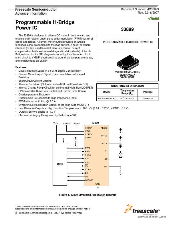
VDDL +5.0 V VIGNP
VIGNP VCC VDDQ CSNS REDIS CRES VCCL FWD REV PWM EN1 S0 RS EN2 CS SCLK D1 D0 LSCMP GND S1
Figure 1. 33899 Simplified Application Diagram
- This document contains certain information on a new product. Specifications and information herein are subject to change without notice.
© Freescale Semiconductor, Inc., 2007. All rights reserved.
INTERNAL BLOCK DIAGRAM ..
INTERNAL BLOCK DIAGRAM
VIGNP
CRES
Charge Pump To Gate Drives M1 M3 S1 Current Sense, Limitation, and Mirror
VCC VCCL CSNS
+3.3 V Internal Regulator
S0 M2 Gate Drives M4 PWM Override
REDIS
LSCMP FWD REV PWM EN1 EN2 VDDQ SCLK CS DI DO
Direction and PWM Control
Baseline Slew Rate Set
RS mand, Fault, and Temperature Register
Temperature Sense and Shutdown
Figure 2. 33899 Simplified Internal Block Diagram
Analog Integrated Circuit Device Data Freescale...