33989
33989 is System Basis Chip manufactured by Freescale Semiconductor.
features
. Also, an Interrupt can be generated, for the MCU, based on CAN bus activity as well as mode changes.
Features
- VDD1: Low Drop Voltage Regulator, Current Limitation, Overtemperature Detection, Monitoring, and Reset Function
- VDD1: Total Current Capability 200 m A
- V2: Tracking Function of VDD1 Regulator. Control Circuitry for External Bipolar Ballast Transistor for High Flexibility in Choice of Peripheral Voltage and Current Supply
- Low Stand-By Current Consumption in Stop and Sleep Modes
- High-Speed 1 MBaud CAN Physical Interface
- Four External High Voltage Wake-up Inputs Associated with HS1 VBAT Switch
- 150 m A Output Current Capability for HS1 VBAT Switch Allowing Drive of External Switches Pull-Up Resistors or Relays
- VSUP Failure Detection
- 40 V Maximum Transient Voltage
- Pb Free designated by suffix code EG
SYSTEM BASIS CHIP WITH HIGH-SPEED CAN
DW SUFFIX EG SUFFIX (PB-FREE) 98ASB42345B 28-PIN SOICW
ORDERING INFORMATION Device MC33989DW/R2
- 40°C to 125°C MCZ33989EG/R2 28 SOICW Temperature Range (TA) Package
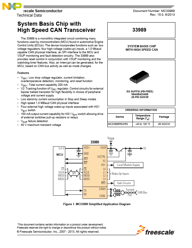
5.0 V MCU VDD1 GND RST INT CS SCLK MOSI MISO CS SCLK MOSI MISO V2CTRL V2 HS1 L0 L1 L2 L3 WD CANH CANL VSUP
VPWR V2
Local Module Supply Wake-Up Inputs Safe Circuits Twisted Pair CAN Bus
TX RX
Figure 1. MC33989 Simplified Application Diagram
Freescale Semiconductor, Inc. reserves the right to change the detail specifications, as may be required, to permit improvements in the design of its products.
© Freescale Semiconductor, Inc., 2007. All rights reserved.
INTERNAL BLOCK DIAGRAM
INTERNAL BLOCK DIAGRAM
VSUP Monitor Dual Voltage Regulator VDD1 Monitor V2CTRL V2 VDD1 HS1 Control HS1 L0 L1 L2 L3 TX RX CAN H CAN L High Speed 1.0 MB/s CAN Physical Interface SPI Interface Programmable Wake-Up Inputs Oscillator Interrupt Watchdog Reset INT WD RST Mode Control CS SCLK MOSI MISO GND
VSUP
V2
Figure 2. 33989 Simplified Internal Block Diagram
Analog Integrated Circuit Device Data Freescale Semiconductor
PIN...