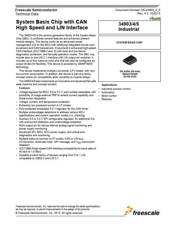
MC34903CP3EKR2
MC34903CP3EKR2 is System Basis Chip - SBC manufactured by Freescale Semiconductor.
- Part of the MC34904C5EKR2 comparator family.
- Part of the MC34904C5EKR2 comparator family.
Freescale Semiconductor Technical Data
Document Number: MC34903_4_5 Rev. 4.0, 10/2013
System Basis Chip with CAN High Speed and LIN Interface
I3n34d49u90s03t3/r4/i/a5l
The 34903/4/5 is the second generation family of the System Basis Chip (SBC). It bines several Features and enhances present module designs. The device works as an advanced power management unit for the MCU with additional integrated circuits such as sensors and CAN transceivers. It has a built-in enhanced high-speed CAN interface (ISO11898-2 and -5) with local and bus failure diagnostics, protection, and fail-safe operation modes. The SBC may include zero or one LIN 2.1 interface with LIN output pin switches. It includes up to four wake-up input pins that can also be configured as output drivers for flexibility. This device is powered by SMARTMOS technology.
SYSTEM BASIS CHIP
This device implements multiple Low-power (LP) modes, with very low-current consumption. In addition, the device is part of a family concept where pin patibility adds versatility to module design.
EK Suffix (Pb-free) 98ASA10556D 32-PIN SOIC
The 34903/4/5 also implements an innovative and advanced fail-safe state machine and concept solution.
Applications
Features
- Industrial process control
- Voltage regulator for MCU, 5.0 or 3.3 V, part number selectable, with possibility of usage external PNP to extend current capability and share power dissipation
- Voltage, current, and temperature protection
- Automation
- Motor control
- Robotics
- Extremely low quiescent current in LP modes
- Fully-protected embedded 5.0 V regulator for the CAN driver
- Multiple undervoltage detections to address various MCU specifications and system operation modes (i.e. cranking)
- Auxiliary 5.0 or 3.3 V SPI configurable regulator, for additional ICs, with overcurrent detection and undervoltage protection
- MUX output pin for device internal analog signal monitoring and power supply monitoring
- Advanced SPI, MCU, ECU power...


