Datasheet4U Logo Datasheet4U.com

MC34904C3EK - System Basis Chip - SBC

This page provides the datasheet information for the MC34904C3EK, a member of the MC34904C5EKR2 System Basis Chip - SBC family.

Description

31 Introduction 31 Functional Pin Description 31 Functional Device Operation 35 Mode and State Description 35 LP Modes 36 State Diagram 37 Mode Change 38 Watchdog Operation 38 Functional Block Operation Versus Mode 40 Illustration of Device Mode Transitions.

Features

  • and enhances present module designs. The device works as an advanced power management unit for the MCU with additional integrated circuits such as sensors and CAN transceivers. It has a built-in enhanced high-speed CAN interface (ISO11898-2 and -5) with local and bus failure diagnostics, protection, and fail-safe operation modes. The SBC may include zero or one LIN 2.1 interface with LIN output pin switches. It includes up to four wake-up input pins that can also be configured as output drivers.

📥 Download Datasheet

Datasheet preview – MC34904C3EK

Datasheet Details

Part number MC34904C3EK
Manufacturer Freescale Semiconductor
File Size 954.62 KB
Description System Basis Chip - SBC
Datasheet download datasheet MC34904C3EK Datasheet
Additional preview pages of the MC34904C3EK datasheet.
Other Datasheets by Freescale Semiconductor

Full PDF Text Transcription

Click to expand full text
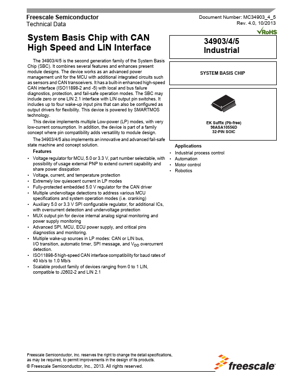
Freescale Semiconductor Technical Data Document Number: MC34903_4_5 Rev. 4.0, 10/2013 System Basis Chip with CAN High Speed and LIN Interface I3n34d49u90s03t3/r4/i/a5l The 34903/4/5 is the second generation family of the System Basis Chip (SBC). It combines several features and enhances present module designs. The device works as an advanced power management unit for the MCU with additional integrated circuits such as sensors and CAN transceivers. It has a built-in enhanced high-speed CAN interface (ISO11898-2 and -5) with local and bus failure diagnostics, protection, and fail-safe operation modes. The SBC may include zero or one LIN 2.1 interface with LIN output pin switches. It includes up to four wake-up input pins that can also be configured as output drivers for flexibility.
Published: |