MCZ33399
MCZ33399 is Local Interconnect Network (LIN) Physical Interface manufactured by Freescale Semiconductor.
features of CAN are not required. The 33399 is a Physical Layer ponent dedicated to automotive sub-bus applications. It offers speed munication from 1.0 kbps to 20 kbps, and up to 60 kbps for Programming Mode. It has two operating modes: Normal and Sleep. The 33399 supports LIN Protocol Specification 1.3. Features
- Nominal Operation from VSUP 7.0 V to 18 V DC, Functional up to 27 V DC Battery Voltage and Capable of Handling 40 V During Load Dump
- Active Bus Waveshaping to Minimize Radiated Emission
- ± 5.0 k V ESD on LIN Bus Pin, ± 4.0 k V ESD on Other Pins
- 30 kΩ Internal Pullup Resistor
- Ground Shift Operation and Ground Disconnection Fail-Safe at Module Level
- An Unpowered Node Does Not Disturb the Network
- 20 µA in Sleep Mode
- Wake-Up Capability from LIN Bus, MCU mand and Dedicated High Voltage Wake-Up Input (Interface to External Switch)
- Interface to MCU with CMOS-patible I/O Pins
- Control of External Voltage Regulator
- Pb-FREE packaging designated by package code EF
LIN PHYSICAL INTERFACE
D SUFFIX EF SUFFIX (PB-FREE) 98ASB42564B 8 PIN SOICN
ORDERING INFORMATION
Device MC33399D/R2
- 40°C to 125°C MCZ33399EF/R2 8 SOICN Temperature Range (TA) Package
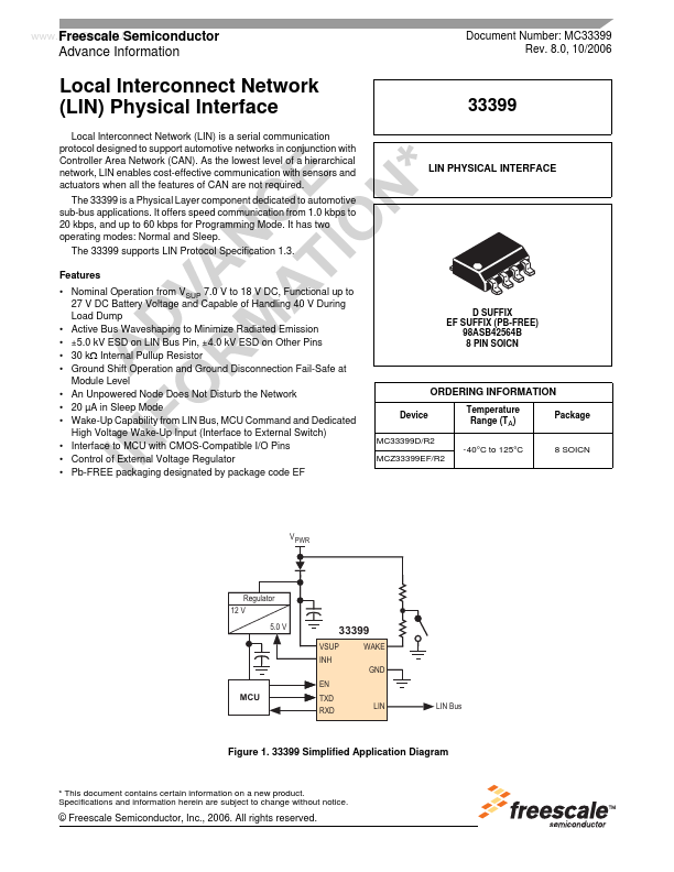
V PWR
Regulator 12 V 5.0 V
VSUP INH EN WAKE GND
TXD RXD
LIN Bus
Figure 1. 33399 Simplified Application Diagram
- This document contains certain information on a new product. Specifications and information herein are subject to change without notice.
© Freescale Semiconductor, Inc., 2006. All rights reserved.
INTERNAL BLOCK DIAGRAM
INTERNAL BLOCK DIAGRAM
WAKE
VSUP
INF EN
Wake-Up VREG Control
VREF Bias
30 kΩ
Logic
RXD Protection
Receiver...