MMA5148AKWR2 Overview
Figure 2. Device Orientation Diagram Z: -1g MMA51xxAKW 2 Sensors Freescale Semiconductor, Inc. Internal Block Diagram VCC CS SCLK DIN DOUT SPI Buffer Voltage Regulator VBUF Reference VREF Voltage Digital Voltage Regulator VREG Analog Voltage Regulator VREGA VBUF Low Voltage Detection Control Logic OTP Array Sync Pulse Detection Programming Interface Serial Encoder Self-Test Interface g-cell VREG VREGA VREG ΣΔ Converter Control Status In Out DSP SINC Filter IIR LPF pensation Offset Monitor HPF Figure 3. Block Diagram VBUF VREG VREGA VSSA
MMA5148AKWR2 Key Features
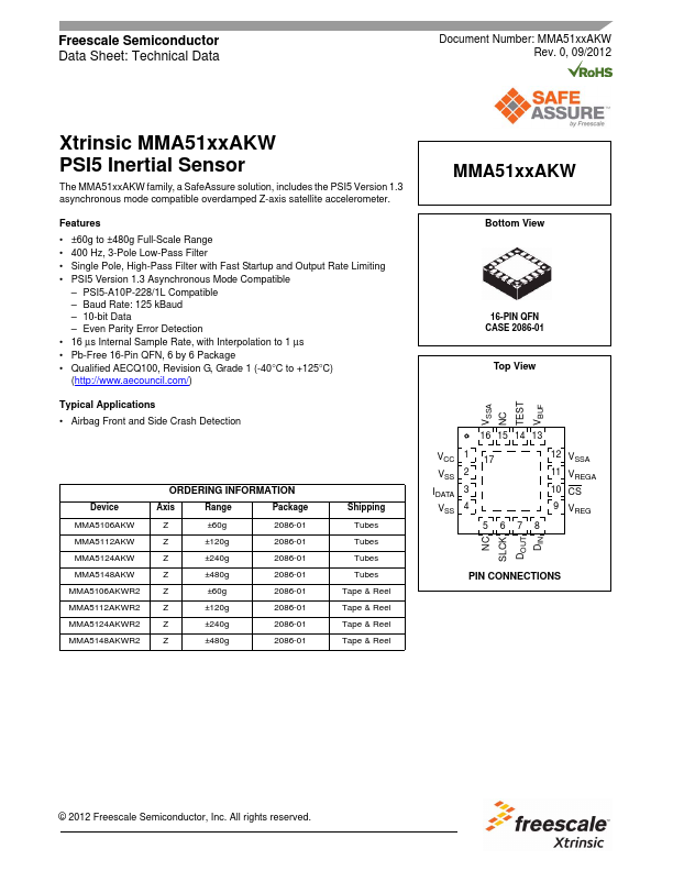
- ±60g to ±480g Full-Scale Range
- 400 Hz, 3-Pole Low-Pass Filter
- Single Pole, High-Pass Filter with Fast Startup and Output Rate Limiting
- PSI5 Version 1.3 Asynchronous Mode patible
- PSI5-A10P-228/1L patible
- Baud Rate: 125 kBaud
- 10-bit Data
- Even Parity Error Detection
- 16 μs Internal Sample Rate, with Interpolation to 1 μs
- Pb-Free 16-Pin QFN, 6 by 6 Package