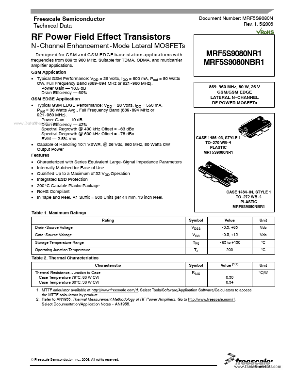
Datasheet4U Logo Datasheet4U.com

MRF5S9080NR1 - GSM/GSM EDGE LATERAL N-CHANNEL RF POWER MOSFETs

General Description

4.7 μF Chip Capacitors (1812) 10 nF 200B Chip Capacitors 33 pF 600B Chip Capacitors 22 pF 600B Chip Capacitors 1.8 pF 600B Chip Capacitor 9.1 pF 600B Chip Capacitor 8.2 pF 600B Chip Capacitors 10 pF 600B Chip Capacitors 4.7 pF 600B Chip Capacitor 3.6 pF 600B Chip Capacitor 220 μF, 63 V Electrolytic

Key Features

  • Characterized with Series Equivalent Large - Signal Impedance Parameters.
  • Internally Matched for Ease of Use.
  • Qualified Up to a Maximum of 32 VDD Operation.
  • Integrated ESD Protection.
  • 200_C Capable Plastic Package.
  • RoHS Compliant.
  • In Tape and Reel. R1 Suffix = 500 Units per 44 mm, 13 inch Reel. Table 1. Maximum Ratings Rating Drain- Source Voltage Gate- Source Voltage Storage Temperature Range Operating Junction Temperature Symbol V.

📥 Download Datasheet

Full PDF Text Transcription (Reference)

The following content is an automatically extracted verbatim text from the original manufacturer datasheet and is provided for reference purposes only.

View original datasheet text
Freescale Semiconductor Technical Data Document Number: MRF5S9080N Rev. 1, 5/2006 RF Power Field Effect Transistors N - Channel Enhancement - Mode Lateral MOSFETs Designed for GSM and GSM EDGE base station applications with frequencies from 869 to 960 MHz. Suitable for TDMA, CDMA, and multicarrier amplifier applications. GSM Application • Typical GSM Performance: VDD = 26 Volts, IDQ = 600 mA, Pout = 80 Watts CW, Full Frequency Band (869 - 894 MHz or 921 - 960 MHz). Power Gain — 18.5 dB Drain Efficiency — 60% GSM EDGE Application • Typical GSM EDGE Performance: VDD = 26 Volts, IDQ = 550 mA, Pout = 36 Watts Avg., Full Frequency Band (869 - 894 MHz or 921 - 960 MHz). Power Gain — 19 dB www.DataSheet4U.